Circuit Diagram
Index 645
SAMPLER_AND_MULTIPLEXER
Published:2009/7/14 3:29:00 Author:May


Sample of signal input voltage is fed to output when sampling pulse from external digital timing matrix is applied to primary of pulse transformer through Q3.-N. Aron and C. Granger, Analog-To-Digital Converter Uses Transfluxors, Electronics, 35:20, p 62-66. (View)
View full Circuit Diagram | Comments | Reading(714)
NULL_VOLTMETER
Published:2009/7/15 20:20:00 Author:Jessie

Logarithmic voltmeter using Optical Electronics 9818 opamp and 2245C four-decade bipolar logarithmic function can serve as output indicator of Wheatstone bridge, as solid-state galvanometer, or as indicator for differentia[ voltmeter or comparison bridge. Meter scale values are relative; basic sensitivity of circuit corresponds to 1 on scale, representing 100 nV. With this sensitivity, 1 mV gives full-scale reading. Other three positions of range switch give 100 mV, 10 V, and 1000 V for full scale, when using 10-0-10 V meter. Inherent limiting of opamp protects circuit from overvoltage damage.- A Logarithmic Null-Volt-meter Design, Optical Electronics, Tucson, AZ, Application Tip 10084. (View)
View full Circuit Diagram | Comments | Reading(1952)
15_W_POWER_AMPLIFIER_FOR_440_MHz
Published:2009/7/14 3:28:00 Author:May

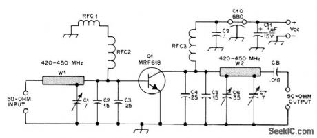
Power gain of 10 dB increases effective range of amateur transmitter. Narrow-band amplifier using Motorola MRF618 internally matched 12.5-V controlled-a transistor can be tuned from 430 to 450 MHz. Multiple L sections using 50-ohm microstrip line and mica compression variable capacitors provide input-match and collector-load transformations. Article gives printed-circuit board layout for U-shaped 0.112-inch-wide stripline inductors W1 and W2. RFC1 is ferrite bead, RFC2 is 8 turns No. 22 enamel closewound on 1/8-inch form, and RFC3 is 4 turns No. 22 enamel closewound on 1/4-inch form.-R. Olsen, Build This Solid-State PA for 440 MHz, QST, Feb. 1977, p 37-38. (View)
View full Circuit Diagram | Comments | Reading(2010)
BALANCED_DIFFERENTIAL_OPERATIONAL_AMPLIFIER
Published:2009/7/15 20:19:00 Author:Jessie

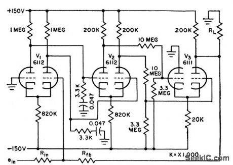
Open-loop gain is above 5,000 into 10,000-ohm load. Good stability and summing accuracy are obtained with closed. loop gains of 0.1 to 100. Provides 50-V out-put voltage swing for integrating or differentiating in control systems. Phase lag of 5° at 20 cps with closed-loop gain of 10 pre dudes use in high-frequency control systems.-L. S. Klivans, D-C Amplifiers for Control Systems, Electronics, 31:47, p 96-100. (View)
View full Circuit Diagram | Comments | Reading(756)
FET_VOLTMETER_1
Published:2009/7/15 20:17:00 Author:Jessie

Performance is comparable to that of vacuum-tube voltmeter, without requirement of AC supply Drift rate is far superior to that of tubes, allowing 0.5-V full-scale range. Uses low-leakage low-noise NPD8303 dual JFET. - FET Databook, National Semiconductor, Santa Clara, CA, 1977, p 6-26-6-36.
(View)
View full Circuit Diagram | Comments | Reading(0)
SAWTOOTH_SYNC_GENERATOR
Published:2009/7/14 3:28:00 Author:May

Provides sync and sawtooth signals for power oscillator control system of induction heater.-R.E. Mathews and E.R. Sias, Jr. , Testing Space Craft with Induction Heaters, Electronics, 35:34. P,38-41. (View)
View full Circuit Diagram | Comments | Reading(912)
DIFFERENTIAL_AMPLIFIER_1
Published:2009/7/15 20:17:00 Author:Jessie

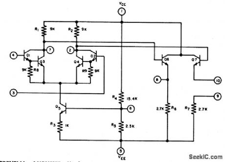
Single-stag e configuration for monolithic construction uses bleeder resistors with Darlington input transistors to increase bandwidth and gain. Current source is biased from separate bias resistor to increase output amplitude. Minimum differential voltage gain of Micronet 203 version is 100 and minimum bandwidth is 500 kc.-C. L. Heizman and D. G. Paterson, Circuit Analysis: A Monolithic Integrated Operational Amplifier, EEE, 13:5, p 80-84. (View)
View full Circuit Diagram | Comments | Reading(787)
_5_V_AT_3_A_SWITCHING
Published:2009/7/14 3:27:00 Author:May

Negative-voltage regulator using SN52104 or SN72304 accepts input voltage range of -8.5 V to -40 V and pro-vides regulated output of -5 V with typical load regulation of 1 mV and input regulation of 0,06%. ICs are interchangeable with LM104 and LM304 respectively. L1 is 60 turns No. 20 on Arnold Engineering A930157-2 molybdenum permalloy core or equivalent.- The Linear and Interface Circuits Data Book for Design Engineers, Texas Instruments, Dallas, TX, 1973, p 5-5. (View)
View full Circuit Diagram | Comments | Reading(764)
HIGH_INPUT_IMPEDANCE
Published:2009/7/15 20:16:00 Author:Jessie

All transistors are on RCA CA3095 transistor array. Q1-Q4 are connected to form bridge, with voltage to be measured applied to base 9. Circuit balance and calibration are achieved by varying DC voltage applied to base of a2. Q7 and O8 serve as constant-current source for cascode differential amplifier connection of Q1-Q4. Differential out-put of bridge is applied to differential input of CA3748 opamp driving meter. Switch gives choice of three voltage ranges,-E. M. Noll, Linear IC Principles, Experiments, and Projects, Howard W. Sams, Indianapolis, IN, 1974, p327.
(View)
View full Circuit Diagram | Comments | Reading(0)
CODING_DIGIT_CARD
Published:2009/7/14 3:27:00 Author:May

Initiate pulse starts coding in digit card of analog-digital converter and ultimately provides positive shift-carry pulse for next card. Codes inputs up to 5 v at maximum sampling rate of 5,000 inputs per second with 0.5% accuracy. Eight binary-digit result is shifted out serially at 100,000 digits per second.-W. B. Towles, Transistorized Analog-Digital Converter, Electronics,31:31, p 90-93. (View)
View full Circuit Diagram | Comments | Reading(590)
ELECTROSCOPE
Published:2009/7/15 20:15:00 Author:Jessie

Gate of FET floats, being connected only to smooth metal rod tipped with polished brass ball. Rod is insulated from housing with polystyrene washer in large hole. Static drain current of FET is balanced out of meter with R2 when ball is clear of operator's body or other object. Meter deflection then is proportional to intensity of charge on body brought near ball and on separation. Electroscope will respond to vigorously stroked paper or just-used comb.-R. P. Turner, FET Circuits, Howard W. Sams, Indianapolis, IN, 1977, 2nd Ed., p 153-154. (View)
View full Circuit Diagram | Comments | Reading(4693)
2712_MC_DIELECTRIC_HEATER
Published:2009/7/14 3:27:00 Author:May

Pulse-controlled frequency-stabilization servo mechanism retunes self-excited power oscillator continually, with 200-cps mvbr governing rate at which system compares oscillator frequency with that of crystal-controlled reference oscillator.-J. Markus and V. Zeluff, Handbook of Industrial Electronic Control Circuits, McGraw-Hill, N.Y., 1956, p 173. (View)
View full Circuit Diagram | Comments | Reading(870)
MULTIPLIER_DIVIDER
Published:2009/7/14 3:25:00 Author:May

Upper half of circuit is log converter in which output at A1 is logarithmic ratio of E1 and E2. A3 and Q3 form second log converter for E3 input. Log output of second converter is added to that of upper circuit, producing log (E1 E3 /E2) at emitter of Q4.Q4 and A4 take antilog to give final output equal to E1 E3 / 10E2. If only multiplication is desired, E2 can be reference voltage; R4will then establish reference current.-W.G. Jung,″IC Oρ-Amp Cookbook,''Howard W Sams,Indianapolis,IN,1974,p 216-217. (View)
View full Circuit Diagram | Comments | Reading(0)
ANALOG_SAMPLE_HOLD_CIRCUIT
Published:2009/7/14 3:25:00 Author:May

Uses diode bridge as switching circuit. Operational amplifier A delivers maximum current of 10 ma. Chopper-stabilized operational amplifier B delivers 100 v at 10 ma.-T. A. Brubaker, Precision Analog Memory Has Extended Frequency Response, Electronics, 34:39,p 141-143. (View)
View full Circuit Diagram | Comments | Reading(715)
DIGITAL_BURST_GENERATOR_
Published:2009/7/14 3:25:00 Author:May


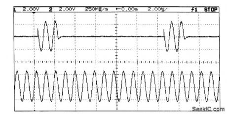
Figure 1 illustrates the transmitted signal and the continuous sine wave from which it is derived. Because the HA4600 buffer has an enable/disable feature, it will pass or reject the input waveform, depending on the state of the enable pin (Fig. 2.). The input signal also is present at the input to the HFA3046 transistor array, which has been configured as a high-speed, high-gain comparator. The comparator squares up the input signal and applies it to the inputs of the two counters, X and Y. The X counter controls the buffer enable, and it determines how many cycles of the input waveform get passed to the output. The four switches SX0 through SX3 are binary-coded. Consequently, if two switches (SX0=1 cycle and SX3=2 cycles) are closed, three cycles of the input sine wave will be passed to the output. Furthermore, the input signal is connected to the Y counter, which controls the repetition rate by determining the OFF period between pulse bursts. The four switches SY0 through SY3 are binary-coded. When all of these switches are closed, the OFF period will be 16 times the period of the input waveform. With the X and Y counters set as described earlier, the repetition rate is the reciprocal of (16+3) times the period of the incoming waveform. If a longer repetition rate is desired, a flip-flop or another counter can be added in series with the output of the Y counter to extend the OFF time. R6, R7, and R8 bias the long-tailed transistor at 10 mA, which is the optimum point for speed. R5 and R6 are small enough to discharge quickly, thus preventing saturation. Configured as shown, the circuit will handle 10-MHz input signals with little degradation. The limit on frequency response is the speed of the logic and the comparator delay time. The comparator delay time can be eliminated by one-shotting out the delay. (View)
View full Circuit Diagram | Comments | Reading(1456)
ISOLATION_OSCILLATOR
Published:2009/7/14 3:25:00 Author:May


Used to isolate duty-cycle generator induction heater control system from pulser of power oscillator.-R.E.Mathews and F. R. Siad, Jr., Testing Space Craft with Induction Heaters,Electronics,35:34,p 38-41. (View)
View full Circuit Diagram | Comments | Reading(812)
ELEPHONE_BELL_INDICATOR_CIRCUIT
Published:2009/7/14 3:25:00 Author:May

This circuit uses a 555 timer to gate an SCR. The SCR passes 12 V to an alarm bell. The bell should be of the mechanical interrupter type so that it will reset and ring only when ring signals are on the telephone line. (View)
View full Circuit Diagram | Comments | Reading(2795)
HIGH_VOLTAGE_POSITIVE_SWITCHING
Published:2009/7/14 3:24:00 Author:May

Uses 18-V zener in series with 3.9K resistor to provide power for LM305 IC regulator. Q2 provides base drive for PIC626 hybrid power switch and isolates output of LM305 from switch.-L. Dixon and R. Patel, Designers' Guide to: Switching Regulators, EDN Magazine, Oct. 20, 1974, p 53-59. (View)
View full Circuit Diagram | Comments | Reading(832)
TEMPERATURE_COMPENSATED_DECODER
Published:2009/7/14 3:24:00 Author:May

Matched diodes in ladder-type network decoder change one reference voltage of transistor switch to compensate for temperature effects-C. R. Pearman and A. E. Popodi, How to Design High-Speed D-A Converters,Electronics,37:8,p 28-32. (View)
View full Circuit Diagram | Comments | Reading(576)
PULSE_WIDTH_TO_ANALOG_DEMODULATOR
Published:2009/7/14 3:23:00 Author:May

Circuit integrates incoming pulse and holds final value until next pulse arrives, Output then returns to zero for next integration. Output range is 0 to 10 v for input pulse width range of 0 to 1 microsec.-D. Knowlton, Modulated Pulse Width Converted to Analog Voltage, Electronics, 38:20, p 99-100. (View)
View full Circuit Diagram | Comments | Reading(834)
| Pages:645/2234 At 20641642643644645646647648649650651652653654655656657658659660Under 20 |
Circuit Categories
power supply circuit
Amplifier Circuit
Basic Circuit
LED and Light Circuit
Sensor Circuit
Signal Processing
Electrical Equipment Circuit
Control Circuit
Remote Control Circuit
A/D-D/A Converter Circuit
Audio Circuit
Measuring and Test Circuit
Communication Circuit
Computer-Related Circuit
555 Circuit
Automotive Circuit
Repairing Circuit