
Circuit Diagram
Index 644
AUTOMATIC_POLARITY_SWITCHING
Published:2009/7/15 20:37:00 Author:Jessie

Can be added to almost any high-impedance voltmeter to give automatic reversal of polarity as required during measurements. Additional contacts on relay can be used to switch polarity indicators. FET input prevents meter shunting. Feedback is used in opamp comparator to speed switching action.-H. Wedemeyer, Auto Polarity Switching for Voltmeters, Wireless World, Oct. 1974, p 380.
(View)
View full Circuit Diagram | Comments | Reading(1593)
INDUCTION_HEATER_POWER_OSCILLATOR
Published:2009/7/14 3:30:00 Author:May

Circuit includes power supplies for oscillator and keyer bias.-R. E. Mathews and F. R.Sias, Jr., Testing Space Craft with Induction Heaters, Electronics, 35:34. P,38-41. (View)
View full Circuit Diagram | Comments | Reading(2990)
CHANNEL_SELECTOR_REPLACES_TUNING_DEVICES
Published:2009/7/15 20:36:00 Author:Jessie

By sensing leading edges of input signal, discriminator having two monostable multivibrators, inverter, and two and gates provides output for desired channel frequency in radio, television, telemetry, and digital control systems.-J. H. Firestone, Gated Pulses Yield Selected Frequency Outputs, Electronics, 36:51, p 38-40. (View)
View full Circuit Diagram | Comments | Reading(578)
FET_AC_VOLTMETER
Published:2009/7/15 20:36:00 Author:Jessie

Covers 0-1000 VRMS in eight ranges. Frequency response referred to 1 kHz is down 3.5 dB at 50 Hz and down 2 dB at 50 kHz. Meter deflection is proportional to average value of AC signal voltage, but meter can be calibrated to read RMS voltages on sine-wave basis. Use 1% resistors for voltage divider. Useful for audio and ultrasonic measurements and tests.-R. P. Turner, FET Circuits, Howard W. Sams, Indianapolis, IN, 1977, 2nd Ed., p 122-124. (View)
View full Circuit Diagram | Comments | Reading(1172)
PHASE_DISCRIMINATOR
Published:2009/7/15 20:35:00 Author:Jessie

Will deliver half-wave pulses to one of two loads, as determined by 0 or 180° difference between input signal and reference source. Useful where different devices, such as heating and cooling equipment, are to be actuated by change of signal phase.-A Phase Discriminator, Electronic Circuit Design Handbook, Mactier Pub. Corp. N.Y.1965, p 88. (View)
View full Circuit Diagram | Comments | Reading(1399)
3SUP3_SUP_SUB4_SUB_DIGIT_METER
Published:2009/7/15 20:35:00 Author:Jessie

National MM5863 12-bit binary building binary block is used with LF13300 analog section of A/D converter to provide ±8191 counts on NSB3881 display MM74C926 CMOS counter is connected to count clock pulses during ramp reference cycle of LF13300. Counts are latched into display when comparator output trips and goes low Operates from single 15-V supply with aid of DC/DC converter LM555 serves as clock and generates required negative supply voltages All diodes are 1N914. -″MOS/LSI Data Databook,″National Semiconductor, Santa Clara, CA, 1977, p 5-2-5-22. (View)
View full Circuit Diagram | Comments | Reading(2216)
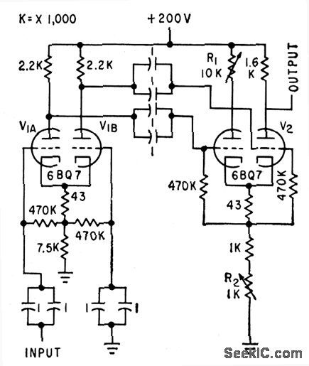
INTEGRATED_CIRCUIT_DIFFERENTIAL_AMPLIFIER
Published:2009/7/15 20:32:00 Author:Jessie
Common-mode output is 0.5mV peak-to-peak, differential gain is 540, and common-mode rejection is 120 db at 60 cps in Amelco D13001: monolithic integrated circuit.-T. Prosser, How to Measure Differential. Amplifier Common-Mode Rejection, EEE, 12:7, p 74-75. (View)
View full Circuit Diagram | Comments | Reading(683)
VARIABLE_GAIN_DIFFERENTIAL
Published:2009/7/15 20:30:00 Author:Jessie
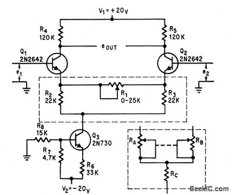
R1 controls gain. High dynamic impedance of constant-current source gives differential amplifier Q1-Q2 high common-mode rejection ratio.-G. Beene, Variable Resistor Controls Differential Amplifier Gain, Electronics, 37:29, p74. (View)
View full Circuit Diagram | Comments | Reading(713)
FET_VOLTMETER_2
Published:2009/7/15 20:30:00 Author:Jessie

Voltage divider provides 22-megohm resistance for FET version of VTVM. JFET Q, is used as source follower, Meter is connected in bridge that is balanced with 1K zero-adjust pot. With proper selection of R, pot can also be used to set zero point of circuit to half scale. Accuracy depends primarily on divider chain. Total current drain rarely exceeds 1 mA, giving long life for almost any type of battery.- I. Math, Math's Notes, CQ, Oct. 1974, p 26-27. (View)
View full Circuit Diagram | Comments | Reading(1396)
AC_LINE_POLARITY_METER
Published:2009/7/15 20:29:00 Author:Jessie

Used to determine correctness of ground wiring in receptacle. Circuit compares voltage waveform on line conductors with AC potential of 10-40 V at 60 Hz picked up by antenna which can be human body. Circuit is synchronous demodulator that conducts on alternate half-cycles depending on whether gate voltage of JFET is positive with respect to source or drain. Zero-center DC milliammeter serves as readout. If plug is inserted into receptacle having balanced power line, milliammetet stays at center to indicate lack of ground. With properly grounded receptacle, meter swings full scale in either direction.-T. Gross, Indicator Shows Correct Wiring Polarity, EDN Magazine, Oct. 20, 1978, p 150 and 152. (View)
View full Circuit Diagram | Comments | Reading(1410)
04_200_MHz_VM
Published:2009/7/15 20:27:00 Author:Jessie

Battery-operated RF voltmeter has full-scale ranges from 0.03 V to 10 V and flat frequency response from 40 kHz to over 200 MHz. Circuit uses voltage-doubling rectifier-type probe CR1-CR2 followed by high-gain DC amplifier driving milliammeter. Article covers construction and calibration in detail.-J. M. Lomasney, Sensitive RF Voltmeter, 73 Magazine, Dec. 1973, p 53-62. (View)
View full Circuit Diagram | Comments | Reading(4531)
POLARITY_INDICATOR
Published:2009/7/15 20:25:00 Author:Jessie

Q1 and Q2 at input should be Darlington transistors to minimize loading on input signal. With no input, current flows through R1D1 and R2D2 networks on alternate half-cycles, Positive signal at input 1 turns on Q1, shunting sum of current through D3 and lighting positive-indicating LED in diode bridge. Similarly, negative voltage on 1 turns on other LED. Supply requirement of 6.3 VAC can usually be obtained from digital multimeter with which indicator is used.-R. A. Snyder, Simple Polarity Indicator Suits DMM's or DPM's, EDN Magazine, Nov. 5, 1977, p 110. (View)
View full Circuit Diagram | Comments | Reading(1562)
DIFFERENTIAL_AC_SIGNALS
Published:2009/7/15 20:26:00 Author:Jessie
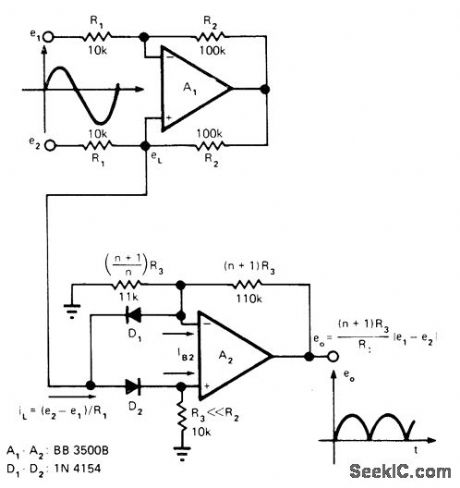
Precision full-wave rectification of differential voltage is achieved by transforming to current for rectification and reconversion to output voltage. One opamp serves as voltage-to-current converter and the other as rectifying current-to-current converter. Circuit is suitable for applications in which lower input impedance and lower frequency response are acceptable. Article gives design equations.-J. Graeme, Measure Differential AC Signals Easily with Precision Rectifiers,. EDN Magazine, Jan, 20, 1975, p 45-48. (View)
View full Circuit Diagram | Comments | Reading(2209)
PHONE_CALL_COUNTER
Published:2009/7/14 3:30:00 Author:May

This circuit counts any string of rings as one call, regardless of duration. If someone hangs up after 1 ring or 10, the counter advances by 1. Similarly, if someone reaches an answering machine and hangs up, or leaves a message, the counter still advances by one call. The counter circuit must ignore signals and react only to the 90-Vac that comes in when the phone is ringing. Because the counter circuit is isolated from the phone line, it needs its own power supply. With some phone systems, power can be pro-vided by the yellow and black wires of the phone line, which typically are connected to a small transformer that provides about 8 Vac. The bridge rectifier Dl to D4, voltage regulator IC1, and filter capacitor C1 convert that to 5 Vdc to power the circuit. If your phone line does not have active yellow and black wires, 6.3 Vac must be connected to the input of the rectifier. Timer IC2 is triggered by relay RY1, which has a coil voltage of about 48 V. Because diode D5 is reverse-biased relative to the normal dc across the phone line, it will pass only partially rectified ac. When the phone rings, D5 passes a partially rectified 90 V, which is enough to energize the relay. Actually, the relay will chatter at about 20 Hz during a ring signal because the rectified voltage is not pure dc. This generates a rapid string of pulses to trigger the timer. But because the timer operates in a retriggerable mode, its output re-mains high for the duration of the rings. The NE555 timer (IC2) is wired in a retriggerable, monostable configuration. The output stays high for a length of time determined by the time constant, 1.1× R2× C2 Because the timer is retriggered with each ring signal, its output will remain high for about 5.5 seconds after the phone stops ringing. The counter will advance by one count whenever the output goes high. Indicator LED1 shows when the phone is ringing and when the output of the timer is high. The high output activates optoisolator IC3 and advances the counter by 1. The counter can be any digital or electromechanical counter whose operation is not affected by the duration of the trigger signal. (View)
View full Circuit Diagram | Comments | Reading(2473)
HARMONIC_MIXER
Published:2009/7/15 20:24:00 Author:Jessie
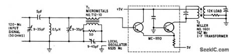
MC-1110 differential amplifier integrated circuit cancels odd-order harmonics while mixing. Local oscillator operates at half of mixing frequency. Conversion gain is 33 db from 120Mc to 10.7 Mc.-R. Hirschfeld. IC'S Improve Differential Amplifiers-and Vice Versa,Electronics.38:16.p75-79. (View)
View full Circuit Diagram | Comments | Reading(0)
REDUCING_24_V_TO_5_V
Published:2009/7/14 3:29:00 Author:May

Uses Fairchild μA78S40 switching regulator having variety of internal functions that can provide differing voltage step-up, step-down, and inverter modes by appropriately connecting external components. Connections shown provide step-down from 24 V to 5 V at 500 mA with 83% efficiency. Applications include running TTL from 24-V battery. Output ripple is less than 25 V. Article gives design equations.-R. J. Apfel and D. B. Jones, Universal Switching Regulator Di-versifies Power Subsystem Applications, Computer Design, March 1978, p 103-112. (View)
View full Circuit Diagram | Comments | Reading(674)
4SUP1_SUP_SUB2_SUB_DIGIT_METER
Published:2009/7/15 20:23:00 Author:Jessie

National MM5330 BCD building block is used with LF13300 analog section of A/D converter to provide ±19,999 counts on NSB5917 display. Circuit contains counters, latches, and multiplexing system for four full digits of display with one decoder/driver, along with sign bit that is valid during overrange and 10,000-count numeral 1, LF13300 has automatic zeroing of all offset voltages. Operation is based on code conversion of number of counts made by MM5330 before comparator crossing is detected. Switch gives choice of 2-, 20-, and 200 V full-scale ranges. Inverters are MM74C14 hex Schmitt triggers. Two-letter NAND gates are MM74C00 CMOS quad NAND gates. One-letter NAND gates (A, B, etc) are DM7400 TTL quad NAND gates.- MOS/LSI Databook, Nation-al Semiconductor, Santa Clara, CA, 1977, p 5-2-5-22.
(View)
View full Circuit Diagram | Comments | Reading(1023)
CANCELLING_POWER_SUPPLY_VARIATIONS
Published:2009/7/15 20:22:00 Author:Jessie
Differential amplifiers in cascade cancel output error caused by supply fluctuations, to permit low-level signal amplification.-J. Holtzman, Reducing Errors Caused by Power-Supply Variations, Electronics, 32:29, p 54-55. (View)
View full Circuit Diagram | Comments | Reading(603)
PTT_LATCH
Published:2009/7/14 3:29:00 Author:May

Eliminates need for holding down microphone switch continuously while transmitting. U1 is inverting hex buffer, and U2 is dual CM0S D flip-flop. When S1 is depressed, input to U1A goes low and its output goes high, making U2A and U1B together turn on Q2 and energize relay K1. Q3-Q5 serve as optional silent power switch for use when relay noise is objectionable.-B. Lambing, DC Latch Circuit, Ham Radio, Aug. 1975, p 42-44. (View)
View full Circuit Diagram | Comments | Reading(862)
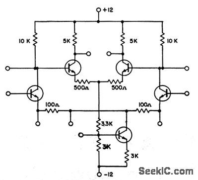
TWO_STAGE_DIFFERENTIAL_AMPLIFIER_WITH_COMMON_MODE_FEEDBACK
Published:2009/7/15 20:21:00 Author:Jessie

Feedback arrangement provides significant reduction in temperature drift of bias circuits. Voltage gains of several thousand are possible.- Transistor Manual, Seventh Edition, General Electric Co. 1964, p 119. (View)
View full Circuit Diagram | Comments | Reading(765)
| Pages:644/2234 At 20641642643644645646647648649650651652653654655656657658659660Under 20 |
Circuit Categories
power supply circuit
Amplifier Circuit
Basic Circuit
LED and Light Circuit
Sensor Circuit
Signal Processing
Electrical Equipment Circuit
Control Circuit
Remote Control Circuit
A/D-D/A Converter Circuit
Audio Circuit
Measuring and Test Circuit
Communication Circuit
Computer-Related Circuit
555 Circuit
Automotive Circuit
Repairing Circuit