
Circuit Diagram
Index 649
NO_CHOPPER_DIFFERENTIAL_AMPLIFIER
Published:2009/7/15 5:21:00 Author:Jessie

Stable voltage gain is 1,000.Current source Q2 provides bias for input stage. Amplification is linear within 10 microvolts over 100℃ range.-D. F. Hilbiber, Stable Differential Amplifier Designed Without Choppers, Electronics, 38:2, p 73-15. (View)
View full Circuit Diagram | Comments | Reading(927)
ANTILOG_CONVERTER
Published:2009/7/14 3:00:00 Author:May

Basic opamp circuit with diode-connected transistor as logging element performs antilog conversion for positive input signals. For negative inputs, roverse transistor connections.-G. B. Clayton, Experiments with Operational Amplifiers, Wireless World, Jan. 1973, p 33-35. (View)
View full Circuit Diagram | Comments | Reading(2135)
DIGITALLY_SELECTABLE_GAIN
Published:2009/7/14 2:59:00 Author:May

TTL controls operation of DG301 low-power analog switch at output of inverting opamp. Low logic gives gain of 1, and high logic gives gain of 10.- Analog Switches and Their Applications, Siliconix, Santa Clara, CA, 1976, p 7-90.
(View)
View full Circuit Diagram | Comments | Reading(728)
2_METER_FOR_10_MHz_IF
Published:2009/7/15 5:20:00 Author:Jessie
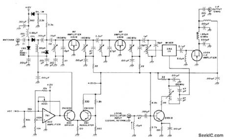
Designed for extreme linearity and selectivity while keeping noise figure below 5 dB Circuit has +15 dBm intercept point and 16-dB power gain, Five tuned circuits at input frequency give overall bandwidth of 4 MHz, with image suppression of 60 dB for 10-MHz IF and 80 dB for 30-MHz IF. Converter uses grounded-gate FET circuit. -U. Rohde, High Dynamic Range Two-Meter Converter, Ham Radio, July 1977,p55-57.
(View)
View full Circuit Diagram | Comments | Reading(1367)
50_MC_SAMPLING_AND_THRESHOLD_CIRCUIT
Published:2009/7/14 2:58:00 Author:May

Threshold tunnel diode receives signal current to be sampled and interrogation pulses repeating at 50 Mc. Diode fires when signal current is below threshold level, making memory tunnel diode switch into its high-voltage state. Current level differences of less than 50 microamp can be resolved in 0.3 nsec, sufficient for converting input into six bits corresponding to 64 levels.-H. R. Schindler, Semiconductor Circuits in a UHF Digital Converter, Electronics, 36:35, p 37-40.
(View)
View full Circuit Diagram | Comments | Reading(747)
INVERTER_BASE_SPEED_UP_WINDINGS
Published:2009/7/15 5:20:00 Author:Jessie

Individual speed-up windings and series capacitors for each transistor base reduce switching times to as little as 4 microsec for 2N174's and to 2 microsec for some germanium power transistors.-A. G. Lloyd, Speed-up Circuits Improve Switching of Transistor Inverters, Electronics, 34:45, p 92-94. (View)
View full Circuit Diagram | Comments | Reading(1029)
LOGAMP
Published:2009/7/14 2:58:00 Author:May

Based on fact that back-to-back diodes driven by current generator give output that varies logarithmically with input signal.With values shown, relation is logarithmic over 60-dB range.Transistors are 2N2924,SK3019,GE-10,or HEP-54,and diodes are 1N914,-Circults,73Magazine, April 1974,ρ 34.
(View)
View full Circuit Diagram | Comments | Reading(889)
PULSE_WIDENER
Published:2009/7/15 5:19:00 Author:Jessie
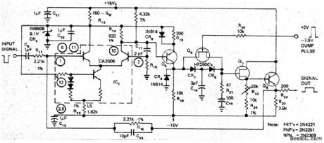
Peak detection diodes CR7 and CR8 in feedback loop of unity-gain CA3006 differential opamp form peak holder that maintains amplitude of narrow video pulses while stretching output pulses as much as 6000 times (from 50 ns to as much as 300 μs). Gain of circuit is unity. Article describes timing and control circuits required in conjunction with peak holder to achieve predictable termination times for stretched pulses, These external circuits include μA710 used as threshold limiter, 9602 dual monostable used as delay-pulse and dump-pulse timing generators, and discrete transistor stage serving as dump-pulse output stage.-B. Pearl, Peak Holder Stretches Narrow Video Pulses, EDN Magazine, Feb. 5, 1973, p 46-47 (View)
View full Circuit Diagram | Comments | Reading(876)
VARIABLE_ON_TIME
Published:2009/7/14 2:57:00 Author:May
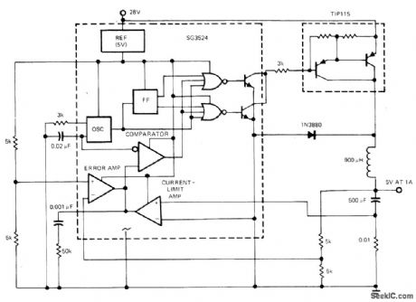
Duty cycle of SG3524 switching regulator is varied by modulating ON time while maintaining constant switching frequency, using pulse- du ration-modulation control circuit.-J. Spencer, Monolithic Switching Regulators-They Fit Today's Power-Supply Needs, EDN Magazine, Sept. 5, 1977, p 117-121.
(View)
View full Circuit Diagram | Comments | Reading(650)
THREE_DIODES_PROVIDE_8_STATES
Published:2009/7/14 2:57:00 Author:May
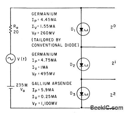
Three different tunnel diodes, each switching at a different input voltage level, act together to convert analog input voltage to digital form.-B. Rabinovici and J. Klapper, Designing Tunnel-Diode Circuits Using Composite Char-acteristics, Electronics, 35:7,p 46-48. (View)
View full Circuit Diagram | Comments | Reading(506)
D_C_AMPLIFIER_SERVES_AS_VOLTAGE_REGULATOR
Published:2009/7/15 5:19:00 Author:Jessie

Output voltage of series pass transistor Q1 is compared to input voltage serving as reference voltage by differential amp liner Q2 and variations are fed back to reduce difference. Feedback ratio of 0.67 gives overall gain of 1.3 and 10-ohm output impedance.-W. S. Zukowsky, Aligning Saturn Missile's Guidance System, Electronics, 37:8, p 26-27. (View)
View full Circuit Diagram | Comments | Reading(730)
400_W__PUSH_PULL
Published:2009/7/14 2:57:00 Author:May
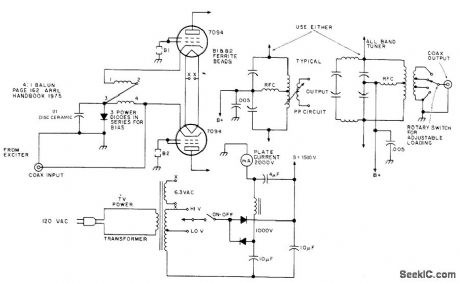
Grounded-grid linear push-pull power amplifier requires no neutralizing, uses balun for push-pull excitation, and can feed either one-band or all-band tuner for amateur radio bands. Balun is 8 turns of 72-ohm twin-line wound on Amidon 2-inch toroid core to give 4:1 ratio. Article covers construction and adjustment.-B Baird, Build This Inexpensive 400 Watt Amplifier, 73Magazine,Holiday issue 1976, p 22-23. (View)
View full Circuit Diagram | Comments | Reading(1266)
160_METER_CONVERTER
Published:2009/7/15 5:17:00 Author:Jessie
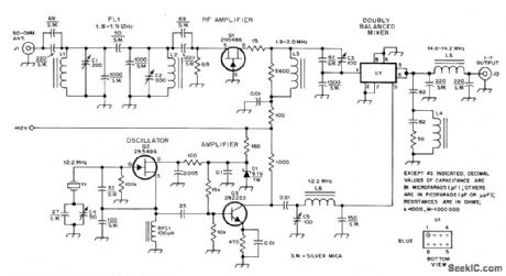
Designed for use with receiver covering 20-meter band. Uses up-conversion techniques to get from 1.8 MHz of 160-meter band to 14-MHz tunable IF of receiver. Butterworth band pass filter at input of converter covers 1.8-1.9 MHz. L1 and L2 each have 31 turns No. 22 enamel on T68-6 toroid core to give 5.1 μH. L3 is 50 μH, using 66 turns No. 18 enamel on T68-1 toroid. Other three coils each use T50-6 toroid core, with L4 having 7 turns No. 24 enamel, L5 11 turns No. 24 enamel, and L626 turns No. 28 enamel. U1 is SRA-1, CM-, or ML-1 diode-quad double-balanced mixer module. -M. Arnold and D. DeMaw, Build This High-Performance Top-Band Converter, QST, Oct. 1978, p 22-24 and 38. (View)
View full Circuit Diagram | Comments | Reading(2951)
RESET_GENERATOR
Published:2009/7/14 2:57:00 Author:May

This VCC monitor circuit draws less than 10μA,yet it can generate reliable RESET signals.
Very low quiescent current makes the reset generator shown suitable for use with microcontrollers that spend most of their time in the “sleep” mode .The system’s power Source,a charged 0.047-μF “Supercap” capacitor(C1),can go without a recharge for intervals exceeding24 hours .The allowable supply-voltage range for the reset circuit is 2 to 11 V. R1 and R2 make it possible to set the switching threshold as low as 1.2 V (the values shown provide a 4.10-V threshold). Hysteresis introduced by R3 minimizes the effect of reference noise and external EMI . Using the values gtven for R2 and R3 (1 MΩ and 10 MΩ),the switching threshold (Vt) is obtained by adjusting the value of R1 alone∶R1 (in megohms)=0.770Vt-0.910. External connections tie the internal reference voltage tothe inverting input of each comparator. Comparator A monitors the supply voltage .When this voltage dips below the threshold established by R1 and R2,the comparator output initiates a RESET pulse via D3 and discharges the timing capacitor (C3)via diode D1. Comparator B determines the pulse duration with help from the time-delay components R4 and C3.Because the duration (approximately 250 ms) is well above the 5-ms mlnlmum required in this case,the effect of supply voltage on pulse width call be ignored . D2 allows the circuit to respond to short outages by providing another quick-discharge path for the timing capacitor. Comparator C is a spare that supplies a complementary output or low-line warnlng. Comparator D acts as an active AND gate for logic-high signals from comparators A and B . The pull-up resistor in many such circuits is 100 kΩ or less (to avoid errors caused by the comparator’s input leakage). In this particular case,it would provide a path for excessive battery discharge during reset. (View)
View full Circuit Diagram | Comments | Reading(739)
16_FUNCTIONS_OF_X_AND_Υ
Published:2009/7/14 2:56:00 Author:May
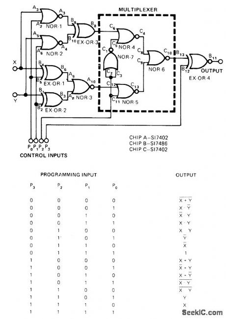
With only three IC chips, circuit provides choice of any one of 16 possible functions of two Boolean variables, Table shows output states for all programming combinations of control inputs P.-S. Murugesan, Programmable Logic Circuit Has Versatile Outputs, EDN Magazine, Feb. 5, 1975,p 57. (View)
View full Circuit Diagram | Comments | Reading(573)
DIRECT_COUPLED_DIFFERENTIAL_AMPLIFIER
Published:2009/7/15 5:17:00 Author:Jessie

Designed for general use as complete amplifier with Darlington output stage, or as first two stages of low-drift high-gain amplifier without amplifier stage. Provides both low and high common. mode rejection for either differential or single-ended outputs. High common-mode rejection is achieved by use of common-mode feedback loop. Low drift is achieved by using dual transistor Q3 as first stage of common-mode feedback loop.-Texas Instruments Inc., Solid-State Communications, McGraw-Hill, N.Y. 1966, p 161. (View)
View full Circuit Diagram | Comments | Reading(779)
140_180_MHz_AT_30_W
Published:2009/7/14 2:55:00 Author:May
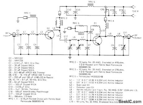
Two-transistor amplifier provides gain of over 20 dB for VHF marine, amateur, and commercial transmitters. Trimmers are tuned for peak output at center frequency in 10-MHz range of interest. Will operate into 30:1 mismatch without damage.-H. Burger and T. Bishop, Two VHF Highband Gain Blocks Form 20-dB, 30-Watt Amplifier Chain, Motorola, Phoenix, AZ, 1975, EB-53. (View)
View full Circuit Diagram | Comments | Reading(2228)
TRANSFORMERLESS_SCR_BRIDGE_INVERTER
Published:2009/7/15 5:17:00 Author:Jessie

Slave-triggering of SCR1 and SCR2 with capacitive load cuts cost in half by eliminating costly gate transformers. Input of 800 pps (both half-cycles of 400-cps mvbr) gives 400-cps sine. wave output with peak amplitude of 350 v, because bridge switching inverts alternate pulses.-L. M. Tibbets, Scr Bridge Inverter Eliminates Transformers, Electronics, 39:18, p 98-99. (View)
View full Circuit Diagram | Comments | Reading(1767)
AF_RECTANGULAR_WAVE
Published:2009/7/15 5:17:00 Author:Jessie

Frequency can be adjusted over wide AF range, with ON and OFF times of rectangular output signal independently varied between 35 and 60% on by choice of values for C1 (0.05to 40 μF), R2 (1K or 2K), and R3 (7.3K to 27K). Minimum value of R3 is 6K.-D.E. Manners, Adjustable Rectangular-Wave Oscillator Interfaces with IC Logic, EDN|EEE Magazine, Sept. 15, 1971, p 46. (View)
View full Circuit Diagram | Comments | Reading(641)
5_V_AT_1_A
Published:2009/7/14 2:55:00 Author:May

National LM122 timer is connected as switching regulator by using internal reference and comparator to drive switching transistor Q1. Minimum input voltage is 5.5 V. Line and load regulation are less than 0.5%, and out-put ripple at switching frequency is only 30 mV. Output voltage can be adjusted between 1 V and 30 V by using appropriate values for R2-R5.-C. Nelson, Versatile Timer Operates from Microseconds to Hours, National Semiconductor, Santa Clara, CA, 1973, AN-97, p 9. (View)
View full Circuit Diagram | Comments | Reading(1360)
| Pages:649/2234 At 20641642643644645646647648649650651652653654655656657658659660Under 20 |
Circuit Categories
power supply circuit
Amplifier Circuit
Basic Circuit
LED and Light Circuit
Sensor Circuit
Signal Processing
Electrical Equipment Circuit
Control Circuit
Remote Control Circuit
A/D-D/A Converter Circuit
Audio Circuit
Measuring and Test Circuit
Communication Circuit
Computer-Related Circuit
555 Circuit
Automotive Circuit
Repairing Circuit