
Circuit Diagram
Index 646
TELEPHONE_LINE_SIMULATOR
Published:2009/7/14 3:23:00 Author:May


When both handsets are on-hook, resistors R1 and R2 supply power to them. When both hand-sets are off-hook, they transmit and receive their own audio. All the TCB does is supply power to them through R1 and R2. If switch S1 is closed, resistor R6 simulates a telephone being plugged into J2, permitting the testing of only one telephone. Now consider the situation where one handset is on-hook and one is off-hook. That causes the on-hook line to go to 24 Vdc and the off-hook line to go to 7 Vdc. The coil of relay RY1 is connected across the two telephone lines, and the voltage difference between the two lines energizes it. When the contacts of RY1 are closed, C2 charges through R4; it takes about 1 second for C2 to charge to 12 Vdc. The 12 Vdc across C2 causes a voltage-controlled switch consisting of R5, Q1, Q2, SCR1, and R8 to close, thus energizing RY2. When RY2 is energized, RY1 is removed from the circuit and a 60-Hz, 37-V p-p sine wave is placed on the telephone lines, causing the telephones to ring. Because RY1 is removed from the circuit, capacitor C2 starts discharging through R7. It takes about 1 second for the capacitor to discharge to about 2.4 Vdc. That lower voltage level causes the voltage-controlled switch to disable RY2, removing the ring voltage from the telephone lines and putting relay RY1 back in the circuit. If one telephone is still off-hook and one is on-hook, the cycle is repeated. (View)
View full Circuit Diagram | Comments | Reading(3352)
COMPARATOR
Published:2009/7/14 3:22:00 Author:May

Comparator action begins when summing and weighting output exceeds analog input and negative pulse is coupled through C1. Trailing edge of blocking oscillator pulse activates reset-rate generator.-W.B. Towles, Transistorized Ancdog-Digital Converter, Electronics, 31:31, p 90-93. (View)
View full Circuit Diagram | Comments | Reading(1322)
CONTROL_FOR_SWITCHING_REGULATOR
Published:2009/7/14 3:19:00 Author:May

Uses all four sections of Motorola MC3302 quad comparator. First section is connected as 20-kHz oscillator that supplies sawtooth output sweeping between voltage limits set by 100K positive feedback resistor and 15-V supply. Section 2 compares sawtooth output to feedback signal, to produce variable-duty-cycle output pulse for power switch of switching regulator. Sections 3 and 4 initiate current-limiting action; section 3 senses over current and triggers section 4 connected as mono MVBR. Limiting occurs at about 4 A. When load short is removed, regulator resets automatically. Point A goes to push-pull drive for power switch of regulator, and point B goes to current-sensing resistor in output circuit of regulator. Point y goes to 10-V supply.-R. J. Bayer, A New Approach to Switching Regulators, Motorola, Phoenix, AZ, 1975, AN-719, p 7. (View)
View full Circuit Diagram | Comments | Reading(844)
TRANSISTORS_FOR_AF_TUBES
Published:2009/7/14 3:19:00 Author:May

Article covers replacement of tubes in Drake T-4XB transmitter with solid-state equivalent circuits mounted in 7-pin and 9-pin miniature plugs,.Numbers identify original tube pins V1A and V2A use dual-cascode JFETs, while- operated transmitter relay control V2B and AM modulator V3 use high-voltage Darlington Q9 collector voltage is set at 150 V during standby by adjusting R9, Circuit includes first and second audio stages. Voltages indicate proper operating points. Source resistors may require adjustment.-H. J. Sartori, Solid-Tubes-a New Life for Old Designs, QST, April 1977, p 45-50.
(View)
View full Circuit Diagram | Comments | Reading(2088)
RANDOM_PULSE_CONVERTER
Published:2009/7/14 3:19:00 Author:May

Transforms random information, as from radiation counter and micrometeorite detector, into analog form suitable for multiplexing, and provides memory between events.-O. B. King, Multiplexing Techniques for Satellite Applications, Electronics, 32:44, p 58-62. (View)
View full Circuit Diagram | Comments | Reading(640)
CONTROLLING_REGULATOR_OUTPUT
Published:2009/7/14 3:18:00 Author:May

Digital control of D/A converter determines output voltage of regulator, with FET serving as voltage-variable resistor. Applications include generation of sequence of voltages for testing components or equipment. Analog Devices MDA-10Z-110 converter generates 0-2 mA output with resolution determined by 10-bit digital input. 741 opamp transforms current to 0-6 V output for varying output of 723 regulator over range of 7-37 V at 150mA maximum.-C. Viswanath, D-A Converter Controls Programmable Power Source, Electronics, July 21, 1977, p 125.
(View)
View full Circuit Diagram | Comments | Reading(1602)
_5_V_FLYBACK_SWITCHING
Published:2009/7/14 3:18:00 Author:May


Uses Unitrode PIC625 regulator operating at 25 kHz and TL497 control circuit operating in current-limiting mode to give line and load regulation of 0.2% for input voltage of 12 V ±25%. Efficiency is 75%. Short-circuit current is automatically limited to 3 A.- Flyback and Boost Switching Regulator Design Guide, Unitrode, Watertown, MA, 1978, U-76, p 5. (View)
View full Circuit Diagram | Comments | Reading(2587)
FM_TELEPHONE_TRANSMITTER
Published:2009/7/14 3:18:00 Author:May

The circuit connects in series with either the tip or the ring (green or red) telephone line. Power for the circuit is full-wave bridge-rectified from the phone line by diodes Dl through D4. Transistor Q1, capacitors C1 and C8, and inductor L3 form an FM oscillator that operates at a frequency of around 93 MHz. Variable capacitor C8 allows the oscillator frequency to be adjusted between 90 and 95 MHz. To move the tuning area up to the 98- to 105-MHz range, C1 must be replaced with a 10-pF capacitor. Audio from the phone line is coupled through R3 and C2 to the base of Q1, where it frequency-modulates the oscillator. Transistor Q3, inductor L1, and capacitor C6 form a power amplifier. The signal tapped off L3 in the oscillator circuit is fed to the base of transistor Q2, and the FM signal is transmitted from Q2's collector. Inductor L2 is a radio-frequency shunt that decouples power and audio from the amplifier circuit. (View)
View full Circuit Diagram | Comments | Reading(150)
POTENTIOMETER_ERROR_COMPUTER
Published:2009/7/14 3:17:00 Author:May

Compensation technique eliminates need for precise high-gain isolation amplifiers when linear potentiometers are used as precision voltage dividers in analog computing circuits. Error is reduced by factor of 100.-M. Kanner, How to Reduce Errors in Loaded Potentiometers, Electronics, 32:34, p 34-35. (View)
View full Circuit Diagram | Comments | Reading(754)
1_2_MHz
Published:2009/7/14 3:17:00 Author:May

Simple low-power AM transmitter uses low-impedance output transformer in reverse to drive 2N107 oscillator stage for shortrange voice transmissions.-Circuits, 73 Magazine, June 1977, p 49. (View)
View full Circuit Diagram | Comments | Reading(752)
TEN_BIT_D_A_CONVERTER
Published:2009/7/14 3:17:00 Author:May

Ten identical stages (three are shown) use selected 2N2501 transistors and matched FA2054 clamping diodes to convert digital signals to equivalent analog voltages for driving servomotors, pen recorders, and deflection circuits of oscilloscopes.-C. R. Pearmcn and A. D. Popodi, How to Design High-Speed D-A Converters, Electronics, 37:8, p 28-32. (View)
View full Circuit Diagram | Comments | Reading(639)
F_M_LIMITER
Published:2009/7/15 20:07:00 Author:Jessie

Four differential-amplifier integrated circuits serve as 60.Mc i-f f-m limiter having 6-Mc bandwidth and 80 db power gain.-R. Hirschfeld, IC's lmproveDifferential Amplifiers-and Vice Versa.Electronics.38:16,p75-79. (View)
View full Circuit Diagram | Comments | Reading(723)
FOUR_STATE_ATTENUATOR
Published:2009/7/14 3:16:00 Author:May

HA-2400 four-channel programmable amplfiier is used as non-inverting four-state attenuator controlled by logic inputs 0 and 1 to D0 and D1. Output voltage for each logic combination is given in truth table. Values shown provide gains of 1, 1/2, 1/4 and 1/8.-W. G. Jung, IC Op-Amp Cookbook, Howard W. Sams, Indianapolis, IN, 1974, p 429-431. (View)
View full Circuit Diagram | Comments | Reading(778)
51_DB_POWER_GAIN_FOR_AUTOPILOT
Published:2009/7/15 20:06:00 Author:Jessie
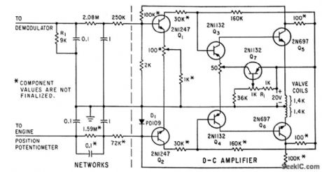
Two differential stages,Q1-Q2 and Q3-Q4,drive two emitter-followers Q5 and Q6 which in turn drive valve coils in pitch and yaw channels of autopilot.-J. H. Porter. Miniaturized. Autopilot System for Missiles.Electronics.33:43,p60-64 (View)
View full Circuit Diagram | Comments | Reading(1511)
ANTILOG_GENERATOR
Published:2009/7/14 3:16:00 Author:May

Basic log generator circuit is rearranged to pelform inverse operation of antilog (exponential) generation. Exponential current generated by O2 is summed at current-to-voltage converter A2.Q1 voltage drive to Q2 is such that collector cument ofQ2 is exponentially related to voltage at base of Q1.Temperature-compensating divider scales input sensitivity to 1V per decade. Feed-forward connections at A1 andA2 optimize circuit for speed.-W. G. Jung, IC 0p-Amp Cookbook, Howard W. Sams, Indianapolis, IN, 1974, p 214-216. ' (View)
View full Circuit Diagram | Comments | Reading(2308)
VOLTAGE_REGULATOR
Published:2009/7/15 20:03:00 Author:Jessie

Portion of three-phase inverter output is filtered, rectified, und compared with temperature-compensated breakdown diode in differential amplifier Q1-Q2. Inverter load current and input battery voltage signals are also fed into differential amplifier, to further improve regulation.-R. J. Kearns and J. J. Rolfe, Three-Phase Static Inverters Power Space-Vehicle Equipment, Electronics, 34:18, p 70-73. (View)
View full Circuit Diagram | Comments | Reading(0)
PREFERRED_BISTABLE
Published:2009/7/15 6:03:00 Author:Jessie

In response to negative trigger, generates voltage steps of opposite polarity at the two outputs. Has no timing function, so second trigger is needed to restore circuit to initial state. Used as radar gate. Requires 150 V plate supply For 6111 and 300 V for 5814A. -NBS, Handbook Preferred Circuits Navy Aeronautical Electronic Equipment, Vol. I, Electron Tube Circuit, 1963, PC 42, p 42-2. (View)
View full Circuit Diagram | Comments | Reading(630)
VOLTAGE_TO_TIME_CONVERTER
Published:2009/7/14 3:16:00 Author:May


Produces output pulse whose width is accurately proportional to unknown input voltage. Pulses are then used to gate clock pulses into digital counters for voltage readout. Conversion occurs each time converter is switched on by monostable mvbr. Thyratron resets counters after each conversion.-B. Bcrker and M. McMahon, Digital Voltmeter Employs Voltage-To-Time Converter, Electronics, 34:18, p 67-69. (View)
View full Circuit Diagram | Comments | Reading(1030)
SUBSCRIBER_LINE_INTERFACE_CIRCUIT_POWER_SUPPLY
Published:2009/7/14 3:15:00 Author:May

A new multiwinding transformer (configurable by the user for a variety of applications) enables an inverting controller to produce the high negative voltages required by an ISDN board or other telephone line card. Such line cards use a subscriber-line interface circuit (SLIC), such as the 79R79 ringing SLIC from AMD. This IC generates the off-hook and on-hook signal transmission, ring-tone generation, and ring-tip detection that constitute an analog telephone interface. For off-hook signal transmission, it requires a tightly regulated -24 or -48 V; to generate ring tones, it requires a loosely regulated -70 V. The five -ringer-equivalent requirement demands 9 to 10 W from the -70-V output, which translates to a full-load lout of about 150 mA. IC1 is an inverting switching regulator that usually converts a 3- to 16-V input to a fixed output of -5 V or an adjustable output. In the circuit shown, three pairs of windings in series (provided by a single off-the-shelf multiwinding transformer) enable IC1 to generate the high voltages needed by a SLIC IC1 (D1). Connecting a diode and output capacitors (C7 and C9) at the first or second pair of windings produces -24 V (as shown) or -48 V, respectively. Feedback to the IC via R1 and R2 achieves tight regulation at this output. The trans-former turns ratios establish a loose regulation at the -70-V output. The circuit can service a five telephone load (10 W) from an input of 12 V, ±10 percent. It operates down to 3 V and produces about 2.4 W at 3.3 V and 3.9 W at 5 V. The -70-V output depends on cross-regulation with respect to the -24-V output. It is, therefore, affected by relative loading on the two outputs (i.e., whether one is heavily loaded and the other lightly loaded, or vice versa). (View)
View full Circuit Diagram | Comments | Reading(1341)
CRYSTAL_CONTROL_IMPROVES_STABILITY
Published:2009/7/15 6:02:00 Author:Jessie

Use of 7-Mc crystal in place of feedback capacitors in conventional mvbr improves stability and waveform while still permitting operation down to 750 kc. Circuit also operates with one crystal; variable 7-47 pf capacitor in noncrystal-controlled side permits varying pulse width on this side over wide range.-H. R. Newhoff, Crystal-Controlled Multivibrator has Better Stability, Electronics, 36:15, p 60-61. (View)
View full Circuit Diagram | Comments | Reading(759)
| Pages:646/2234 At 20641642643644645646647648649650651652653654655656657658659660Under 20 |
Circuit Categories
power supply circuit
Amplifier Circuit
Basic Circuit
LED and Light Circuit
Sensor Circuit
Signal Processing
Electrical Equipment Circuit
Control Circuit
Remote Control Circuit
A/D-D/A Converter Circuit
Audio Circuit
Measuring and Test Circuit
Communication Circuit
Computer-Related Circuit
555 Circuit
Automotive Circuit
Repairing Circuit