
Circuit Diagram
Index 651
DIFFERENTIAL_D_C_AMPLIFIER_CONTROLS_23O_KC_C_W_RADAR_OSCILLATOR
Published:2009/7/15 5:06:00 Author:Jessie

Combined output of two detectors in dual-mode cavity, having typical discriminator S curve, is amp lified by four transistors in differential d-c circuit and applied to oscillator through emitter-follower to make output voltage swing up to 20%. Voltage sextupler applies step-up voltage to reflector of klystron, to maintain klystron frequency constant within 0.2 Mc.-H. D. Raynes, C-W Radar Measures Artillery Ballistics, Electronics, 37:1, p 31-33. (View)
View full Circuit Diagram | Comments | Reading(889)
TV_HORIZONTAL_SWEEP_OSCILLATOR
Published:2009/7/15 5:05:00 Author:Jessie

Cathode-couped multivibrator includes noise-immunizing tuned circuit in plate circuit of 'triode.-C. L. Barsony, Graphical Checkout of Multivibrator Design, Electronics, 33:8, p 55-57. (View)
View full Circuit Diagram | Comments | Reading(1212)
55_MHz_TO_455_kHz
Published:2009/7/15 5:04:00 Author:Jessie
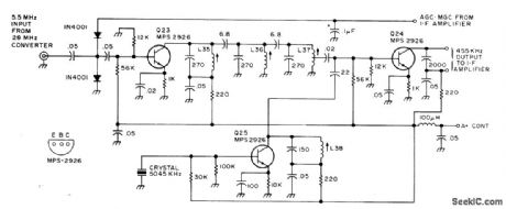
Developed for use as second converter in all-band double-conversion superheterodyne receiver for AM, narrow-band FM CW, and SSB operation. IF amplifier Q23 is followed by triple-tuned filter feeding second mixer Q24, with Q25 as crystal oscillator. Supply is 13.6 V regulated. Article gives all circuits of receiver.-D M Eisenberg, Build This All-Band VHF Receiver, 73 Magazine, Jan, 1975, p105-112 (View)
View full Circuit Diagram | Comments | Reading(3878)
ALIERNATOR_FREQUENCY_CONTROL
Published:2009/7/15 21:02:00 Author:Jessie

Servo discriminator measures phase with respect to preadjusted components, making accuracya function of initial setting. At 400 cps, d-c output is l00 mV for frequency deviation of 0.5 cps. Absolute accuracy is 0.125% between -55 and +100℃ ambient. Used as error-sensing device with servo drive in feedback control loop of constant-speed transmission for aircraft alternators.-R. Hill, Discriminator Controls Aircraft Alternator, Electronics, 31:41, p 94-95. (View)
View full Circuit Diagram | Comments | Reading(665)
0_100000_V_IN_100_μV_STEPS
Published:2009/7/15 21:01:00 Author:Jessie

Constant cur-rent from AD506 opamp drives zener, with 5.16K resistor providing optimum current through zener for temperature-drift cancellation. Chopper-stabilized opamp scales output of zener over full range, Offset-voltage pot serves for zero calibration. Reference voltage is stable to about 11 PPM per year.4. Williams, Don't Bypass the Voltage Reference That Best Suits Your Needs, EDN Magazine, 0ct. 5, 1977, p 53-57. (View)
View full Circuit Diagram | Comments | Reading(1014)
GATED_PULSE_TRAIN
Published:2009/7/15 21:00:00 Author:Jessie
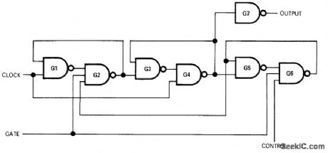
When control is logic 0, circuit transmits train of complete clock pulses to output, beginning with first clock pulse that starts to rise after application of gate signal and ending with last clock pulse that starts before gate signal falls. When control is logic 1, circuit transmits one complete clock pulse after logic 1 gate signal rises. To send another single pulse, gate signal must be removed and reapplied. Gates are Fairchild LPDT μL9047 triple three-input NAND and 9046 quad two-input NAND; other compatible DTL or TTL NAND gates can also be used.-J. V. Sastry, Gated Clock Generates Pulse Train or Single Pulse, EDN|EEE Magazine, July 1, 1971, p 50. (View)
View full Circuit Diagram | Comments | Reading(841)
_5__15_AND__25_V
Published:2009/7/15 21:00:00 Author:Jessie

Stacking of Precision Monolithics REF-02 5-V reference with two REF-01 10-V references gives outputs increasing in steps of 10.000 V from 5,000 V. Any number of additional references can be stacked in same way up to line-voltage limit of 130 V for references, provided total load current does not exceed about 21 mA. Input change from 21 to 55 V produces output change less than noise volt-age of devices in circuit shown.- +5 V Precision Voltage Reference/Thermometer, Precision Monolithics, Santa Clara, CA, 1978, REF-02, p7. (View)
View full Circuit Diagram | Comments | Reading(786)
PULSE_COUNTING_F_M_DISCRIMINATOR
Published:2009/7/15 21:00:00 Author:Jessie
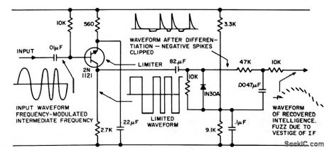
Based on inherent stability of tunnel diode as converter oscillator in f-m receiver for strong-signal locations. Uses 200-kc i-f center frequency as input,-D. Hubbard, Pulse Counter FM Discriminator Design, EEE, 10:7, p 44-49. (View)
View full Circuit Diagram | Comments | Reading(2467)
PRF_DISCRIMINATOR
Published:2009/7/15 20:58:00 Author:Jessie
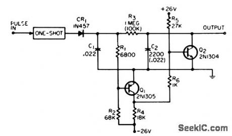
Requires pulse train burst of only two successive pulses to determine prf above or below given limit. Two such circuits with nand gate can indicate presence of given prf within 0.1% or within 1 cps of 1 kc. Input pulses are first given standard width and amplitude by one shot.-G. Richwell, PRF Discriminator, EEE, 13:7, p41. (View)
View full Circuit Diagram | Comments | Reading(733)
BAND_GAP_PRECISION_REFERENCE
Published:2009/7/15 20:58:00 Author:Jessie

Uses diodes from CA3086 array and CA3078 micro-power opamp to develop 2.35-V precisely controlled output reference that is almost indepen-dent of temperature. –″Circuit Ideas for RCA Linear ICs,″RCA Solid State Division, Somerville, NJ, 1977, p 18. (View)
View full Circuit Diagram | Comments | Reading(941)
60_Hz_WITH_50_DUTY_CYCLE
Published:2009/7/15 20:57:00 Author:Jessie
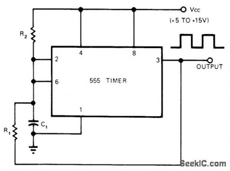
Adding single resistor R2 to standard oscillator connection of 555 timer permits operation with 50% duty cycle independently of frequency as determined by value of C1.For 60-Hz output, VCC is 10 V, C1 is 1 μF, R1 is 10K, and R2 is 75K.-R. Hofheimer, One Extra Resistor Gives 555 Timer 50% Duty Cycle, EDN Magazine, March 5, 1974, p 74-75. (View)
View full Circuit Diagram | Comments | Reading(3153)
5_24_V_SWITCHING
Published:2009/7/14 2:49:00 Author:May

Choice of regulator in μA7800 series determines fixed output voltage. Devices are available for rated outputs of 5, 6, 8, 12, 15, 18, and 24 V, positive or negative, with output current ratings of 100 mA, 500 mA, or 1 A. If input voltage is greater than maximum input rating of regulator used, add voltage-dropping zener Dl to bring voltage between pins 1 and 3 down to acceptable level.- Signetics Analog Data Manual, Signetics, Sunnyvale, CA, 1977, p 668, (View)
View full Circuit Diagram | Comments | Reading(837)
DIGITAL_VOLTMETER_CALIBRATOR
Published:2009/7/14 2:48:00 Author:May
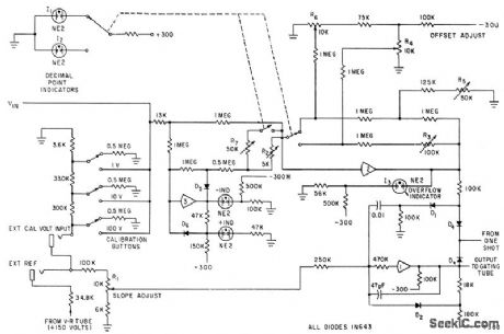
Calibration voltages of 100,10,and 1 V are derived from reference voltage, for use In calibrating digital voltmeter in which analog voltage is converted to pulse whose width is proportional to input amplitude.Used for gating clock pulses into digital counters for voltage readout.-B. Barker and M. McMahan,Digital Voltmeter Employs Voltage-To-Time Converter,Electronics,34:18, p 67-69. (View)
View full Circuit Diagram | Comments | Reading(712)
FM_TELEPHONE_BUG
Published:2009/7/14 2:32:00 Author:May

Q1 is an oscillator tuned to a quiet spot in the FM broadcast band. Dc from the line powers the bug. Connect the gray wire to the phone in place of the green wire, and the green wire on the bug to the green line wire. The red wire goes to the red phone line wire. Audio on the line causes incidental FM, which can be heard on an FM receiver tuned to the frequency of the oscillator. Because this device sees the full line voltage, Q2 is a high-voltage PNP MPSA56 transistor.Warning: Use of this device for certain purposes could violate federal and/or state laws and subject the violator to prosecution. (View)
View full Circuit Diagram | Comments | Reading(2040)
2_W_FOR_20_METER_CW
Published:2009/7/14 2:29:00 Author:May
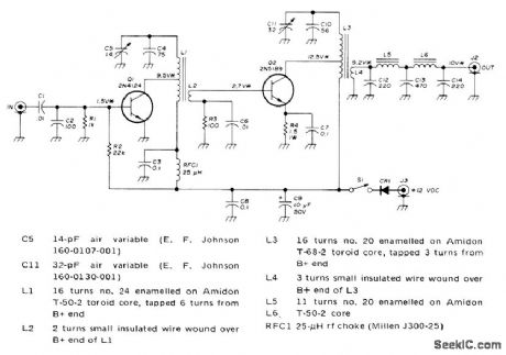
Motorola 2N4124 driver operates as class B amplifier. With no signal, collector current is near zero, minimizing current drain when key is up. Tank circuit of RCA 2N5189 final is similar to that of driver. Double-pi network in output assures good harmonic attenuation. RMS values of BF voltages are marked with asterisks. Protective diode CR1 is any silicon rectifier. For portable use, supply can be lantern battery.-C. E. Galbreath, Low Power Solid-State VFO Transmitter for 20 Meters, Ham Radio, Nov. 1973, p 6-11. (View)
View full Circuit Diagram | Comments | Reading(1648)
LOW_POWER_FM_TELEPHONE_BUG
Published:2009/7/14 2:29:00 Author:May

Q1 (2N3904) is an oscillator tuned to a quiet spot in the FM broadcast band. D1 through D4 (1N914) ensure proper polarity. Dc from the line powers the bug. Audio on the line causes incidental FM, which can be heard on an FM receiver tuned to the frequency of the oscillator. Warning: Use of this device for certain purposes could violate federal and/or state laws and subject the violator to prosecution. (View)
View full Circuit Diagram | Comments | Reading(2623)
120_kHz_TO_4_MHz
Published:2009/7/15 21:17:00 Author:Jessie

Square-wave output of about 3.5 V can be obtained with SN7400 quad NAND gate, quartz crystal of desired frequency, and single resistor. One of unused gates may be used to gate generator output. Insertion of crystal in socket shocks crystal into oscillation at its resonant frequency, for generating square-wave output over most of frequency range. Waveform approaches clipped sine wave near 4 MHz. Output is suitable for triggering SN7490 decade counters reliably, with normal fan-out.-E. G. Olson, 2 Gates Make Quartz Oscillator, EDN Magazine, May 5, 1973, p 74. (View)
View full Circuit Diagram | Comments | Reading(1268)
ANALOG_TYPE_RATIO_COMPUTER
Published:2009/7/15 21:16:00 Author:Jessie

Computes and automatically displays on oscilloscope the ratio of two time-varying quantities, such as noise suppression factor of tube shot noise. Five main parts are sampler, shaper of ramp or step in each channel, amplitude comparator, converter for final indicator, and timing unit that provides sampling signal-J. Tamiya, Automatic Display of Noise Suppression Factor, Electronics, 33:6, p 55-57. (View)
View full Circuit Diagram | Comments | Reading(806)
SQUARE_WAVE_GENERATOR
Published:2009/7/15 21:15:00 Author:Jessie

Uses two 74122 retriggerable mono MVBRs with clear. Two single pots may be used in place of dual 25K pot if up and down times of output must be independently adjustable.-B. Voight, The TTL One Shot, 73 Magazine, Feb. 1977, p 56-58. (View)
View full Circuit Diagram | Comments | Reading(4222)
BINARY_CHANNEL_FOR_EL_DISPLAY
Published:2009/7/15 21:13:00 Author:Jessie

Information is transmitted to decoding unit and display board in series of pulse bursts. each containing entire information to be displayed, for rapid error correction if information is garbled during transmission. System can use pair of wires for transmission, having sufficient bandwidth to pass pulse burst. Information is introduced by opening S9 in transmitter-R. C. Lyman and C. I. Jones, Electroluminescent Panels for Automatic Displays, Electronics, 32:28, p 44-47. (View)
View full Circuit Diagram | Comments | Reading(914)
| Pages:651/2234 At 20641642643644645646647648649650651652653654655656657658659660Under 20 |
Circuit Categories
power supply circuit
Amplifier Circuit
Basic Circuit
LED and Light Circuit
Sensor Circuit
Signal Processing
Electrical Equipment Circuit
Control Circuit
Remote Control Circuit
A/D-D/A Converter Circuit
Audio Circuit
Measuring and Test Circuit
Communication Circuit
Computer-Related Circuit
555 Circuit
Automotive Circuit
Repairing Circuit