
Circuit Diagram
Index 643
±5_V_USING_OPAMP
Published:2009/7/15 20:47:00 Author:Jessie
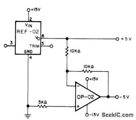
Precision Monolithics REF-02 voltage reference provides +5 V directly, while OP-02 inverting opamp provides -5 V.- +5 V Precision Voltage Reference/Thermometer, Precision Monolithics, Santa Clara, CA, 1978, REF-02, p 6.
(View)
View full Circuit Diagram | Comments | Reading(821)
PRECISION_CURRENT_SOURCE
Published:2009/7/14 3:32:00 Author:May

2N5457 JFET and PN2222 bipolar transistor serve as isolators between output and current-sensing resistor R1. LM101 opamp provides high loop gain to assure that circuit acts as current source.- FET Databook, National Semiconductor、Santa Clara、GA、1977、p6-26-6-36. (View)
View full Circuit Diagram | Comments | Reading(0)
HYDROGEN_THYRATRON_INDUCTION_HEATER
Published:2009/7/14 3:32:00 Author:May


Thyratron acts as high-speed switch, much like spark-gap oscillator, to produce damped oscillations in tank circuit L2-C2.Output frequency is 10 to 14 kc, depending on load. Peak thyratron current is about 340 amp when Vo is 10 kv. Repetition rate depends on maximum average current, and is 124 cps for 0.5 amp. L3 is 0.32 h.-H. L. Van Der Horst, How Radar Techniques Improve Induction Heating, Electronics, 32:7, p 51-55. (View)
View full Circuit Diagram | Comments | Reading(2567)
REFERENCE_SWITCH
Published:2009/7/14 3:32:00 Author:May


Provides low-zero-offset 5-microsec pulses with stabilized amplitude, obtained from synchronous flip-flop. Output pulses switch from zero to -5 v, for driving compute and hold amplifiers of serial decoder,-R. M.Centner and J. R. Wilkinson, New Approach to Serial Decoding Eliminates Static Storage, Electronics, 35:34, p 32-35. (View)
View full Circuit Diagram | Comments | Reading(734)
SIMPLE_PHONE_IN_USE_INDICATOR
Published:2009/7/14 3:32:00 Author:May

The LM741 op amp is used as a voltage comparator, comparing the telephone-line voltage to the battery voltage. The telephone line drops below 9 V when it is in use. That drop turns the op amp on, which lights the LED. Resistor R1 prevents the circuit from loading the telephone line excessively. In my location, the in-use circuit drops the line voltage approximately 5 V. That leaves quite a bit of re-serve because a telephone line operates at approximately 40 to 48 V. Resistor R2 limits the current to the LED. A 1000-Ω resistor will brighten the LED; however, the total circuit current draw will in-crease. The circuit (as shown) consumes 1.15 mA in standby and 3.80 mA when indicating that the line is in use. (View)
View full Circuit Diagram | Comments | Reading(2060)
5_V_TO_200_V_WITH_SWITCHING_REGULATOR
Published:2009/7/14 3:31:00 Author:May

Converts standard logic supply voltage to high voltage required by gas-discharge displays, sing Motorola MC3380 as table MVBR as control element in switching regulator. Will drive up to 15 digits. Operating frequency is about 20 kHz.-H. Wurzburg, Control Your Switching Regulator with the MC3380 As table Multivibrator, Motorola, Phoenix, AZ, 1975, EB-52. (View)
View full Circuit Diagram | Comments | Reading(679)
ADJUSTABLE_REFERENCE
Published:2009/7/15 20:57:00 Author:Jessie

Two-transistor equivalent of zener is combined with Gulton 35TF1 thermistor to give voltage stability within 0.5% over 0-50℃ range, with output voltage adjustable from 3.5 to 15.5 V with R2. Dynamic impedance is only 1 ohm. Developed for regulator service in battery-powered MOS instruments.-R. Tenny, Compensated Adjustable Zener, EDN Magazine, May 5, 1973, p 72. (View)
View full Circuit Diagram | Comments | Reading(748)
_69_V_TO+69_V_VARIABLE
Published:2009/7/15 20:56:00 Author:Jessie

National LM199 temperature-stabilized 6.95-V reference is converted to continuously variable bipolar output by LM108A opamp,Use precision wirewound 10-turn pot. Opamp operates as inverter for negative outputs but is noninverting for positive outputs.- Linear Applications, Vol. 2, National Semiconductor, Santa Clara, CA, 1976, AN-161,p6. (View)
View full Circuit Diagram | Comments | Reading(811)
LOGARITHMIC_RATIO
Published:2009/7/14 3:31:00 Author:May

Output is proportional to logarithm of ratio of input voltages V1 and V2 for voltages between 0 and 10 V. Each input goes to modified logamp circuit using Analog Devices 180K. Outputs are combined by differential opamp (Analog Devices 184L), with Fairchild μA726 temperature -regulated dual transistor serving asfeedback element. Amicle gives design equations and analyzes possible error sources.-D. R. Morgan, Get the Most Out of Log Amplifiers by Understanding the Error Sources, EDN Magazine, Jan. 20, 1973, p 52-55. (View)
View full Circuit Diagram | Comments | Reading(924)
TRANSISTORS_FOR_MIXER_AND_VR_TUBES
Published:2009/7/14 3:31:00 Author:May

Premixer V6 in Drake T-4XB transmitter is replaced by dual-cascode MOSFETs, with CR4 protecting MOSFET from keyed-ground circuit. High-level mixer V7 operates over large dynamic range of signals coming from IF stage Output of mixer is low level, about 4 VRMS maximum. Decoupling capacitor C9 and choke High-level mixer V7 operates over large dynamic range of signals coming from IF stage Output of mixer is low level, about 4 VRMS L1 isolate JFET from high-voltage tube circuit.-H. J. Sartori, Solid-Tubes-a New Life for 0ld Designs, OST, April 1977, p 45-50. (View)
View full Circuit Diagram | Comments | Reading(1425)
VOLTAGE_CONTROLLED_0_1_KC_OSCILLATOR__
Published:2009/7/15 20:51:00 Author:Jessie


Pulse-counting discriminator in feedback loop gives adequate linearity for computing applications. As input voltage rises from 0 to 10 mV, oscillator output frequency rises proportionally.-N. W. Bell and V. Chiunti, Voltage-Controlled Oscillator Uses Negative Feedback,Electronics.35:11,p65-65. (View)
View full Circuit Diagram | Comments | Reading(825)
PHASE_LOCK
Published:2009/7/15 20:48:00 Author:Jessie
Uses flip-flop, filter, and d-c level shift to phase-lock low-frequency oscillator to a desired frequency. Trigger from master frequency source is fed in at B, and trigger from phase-locked frequency is fed to A. Used to sync ujt sawtooth generator to operate at 10 times the 16-cps center frequency at B.-H. Anway, Phase-locked Frequency Discriminator, EEE, 14;3, p 61. (View)
View full Circuit Diagram | Comments | Reading(668)
15_12_V_FOUROUTPUT
Published:2009/7/15 20:46:00 Author:Jessie

Single LM113 1.22-V stable reference is driven by 1-mA FET constant-current source to provide highly stable low-voltage standard driving four adjustable-gain opamps. Gain of each is set to give desired output reference voltage in range from 1.5 to 12 V. Use cermet trimmers and metal-oxide fixed resistors in opamp feedback circuits to achieve stabilities of several millivolts over 0 to 70℃ range.-H. Olson, Two IC's and FET Provide Quad Stable Reference, EDN Magazine, Jan. 20, 1974, p 82.
(View)
View full Circuit Diagram | Comments | Reading(764)
0005_REGULATION
Published:2009/7/15 20:44:00 Author:Jessie

Simple opamp circuit changes less than 1 mV at output for input range of 10-30 V. Circuit is easily modified to give other output voltages, either positive or negative.-M. Walne, High Performance Reference, Wireless World, May 1974, p 123. (View)
View full Circuit Diagram | Comments | Reading(691)
VARIABLE_REFERENCE
Published:2009/7/15 20:43:00 Author:Jessie

With 759 power opamp used as variable-output voltage regulator, output voltage can be varied over full range from zener maximum down to zero by varying voltage from zener. With 791 opamp, voltage can be adjusted down to 2 V. Since output voltage can be less than zener rating, simple boot- 68V strapping cannot be used. Alternate biasing techniques are then required to improve line regulation. Arrangement is capable of supplying several hundred milliamperes while using only low-drift (5 PPM/℃) zener.-R. J. Apfel, Power Op Amps-Their Innovative Circuits and Packaging Provide Designers with More 0ptions, EDN Magazine, Sept. 5, 1977, p 141-144. (View)
View full Circuit Diagram | Comments | Reading(855)
TWO_STAGE_A_F_DISCRIMINATOR
Published:2009/7/15 20:43:00 Author:Jessie

Circuit first shifts phase of incoming signal in proportion to its frequency deviation, then produces d-c voltage proportiotml to phase shift. Used to measure wow and fluller of disk and tape recorders having prerecorded audio signal.-J. F. Delpech, Audio Discriminator Measures Lctrge Frequency Changes, Electronics, 39:9, p 76-77. (View)
View full Circuit Diagram | Comments | Reading(690)
MONO_AND_PRE_DISCRIMI_NATOR
Published:2009/7/15 20:41:00 Author:Jessie

Monoslable multivibrator can be electronically adjusted to vary output pulse width over range of 0.2 microsec to several seconds. By adding feedback path shown in dashed lines, circuit also serves as pulse repetition frequency discriminator in which d.c output voltage is function of frequency front 3 cps to 300 kc.-G. Richwell, Widedlange Monostable, PRF Discriminator, EEE, 13:8, p67. (View)
View full Circuit Diagram | Comments | Reading(506)
REPETITION_RATE_CONTROL
Published:2009/7/14 3:31:00 Author:May
Compensates for fluctuations in repetition rate of hydrogen thyratron in induction heater. Ripple voltage induced in L1 acts on control grid of V1 to displace peaks at which ignition occurs in correct direction to maintain constant repetition rate in damped circuit.-H. L. Van Der Horst, How Radar Techniques Improve Induction Heating, Electronics, 32:7, p 51-55. (View)
View full Circuit Diagram | Comments | Reading(530)
PHASE_DISCRIMINATOR_FOR_A_C_BRIDGE
Published:2009/7/15 20:39:00 Author:Jessie

Amplifed output of cc bridge is compared with ctc reference signal. When both are in phcse, d-c output to recorder is maximum of one polarity. For 180°phase difference, output is maximum of opposite polarity, and is zero for phase-quadrature.-W. A. Rhine-hart and L. Mourlam, FET Performs Well In Balancing Act, Electronics, 38:19, p 88-92 (View)
View full Circuit Diagram | Comments | Reading(776)
RANDOM_NUMBER_GENERATOR
Published:2009/7/14 3:30:00 Author:May
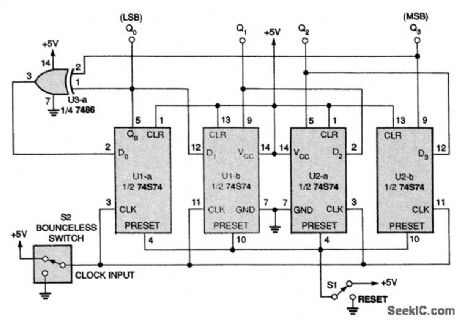
The 74574 flip-flops shown in the circuit are arranged to form a 4-bit shift register. Binary data enter the D0 input on U1-a and are sequentially shifted to each output (Q0, Q1, Q2, Q3) with each clock pulse. The data input to the shift register come from the output of U3-a, one gate of a 7486.That exclusive-OR gate compares two of the output bits from the shift register. If the two bits are the same, then the output of U3-a is 0 Y (or low). If the two bits are different, then the output of U3-a is +5 V (or high). Therefore, U3-a acts as a type of logical-feedback network that changes the data at D0, which, in turn, changes the outputs of the flip-flops. The effect of that network is to create a pseudo-random sequence of bits at the outputs of U1 and U2. (View)
View full Circuit Diagram | Comments | Reading(3056)
| Pages:643/2234 At 20641642643644645646647648649650651652653654655656657658659660Under 20 |
Circuit Categories
power supply circuit
Amplifier Circuit
Basic Circuit
LED and Light Circuit
Sensor Circuit
Signal Processing
Electrical Equipment Circuit
Control Circuit
Remote Control Circuit
A/D-D/A Converter Circuit
Audio Circuit
Measuring and Test Circuit
Communication Circuit
Computer-Related Circuit
555 Circuit
Automotive Circuit
Repairing Circuit