
Circuit Diagram
Index 661
SOLID_STATE_STROBOSCOPE
Published:2009/7/14 1:53:00 Author:May

The schematic diagram for the stroboscope is shown. When switch S2 is closed, a 9-V battery B1 is connected to IC3, a 78L05 voltage regulator, which provides a 5-V source to the circuit. Capacitors C8 and C9 filter the supply. A CD4046 phase-locked loop, IC1, provides a low-frequency square wave to the circuit. Potentiometer R4-a 5000-Ω,10-turn, precision potentiometer with a built-in turns counter-provides a way to adjust and get a direct readout of the FPM rate from 0 to 1000. Switch S1 lets you select the multiplier affecting that rate. Setting S1 to×1, therefore, gives you a 0- to 1000-FPM range, whereas setting S1 to ×10 results in a 0- to 10,000-FPM range. The values of the multiplier settings are determined by capacitors C1 and C2. A 555 timer, IC2, configured in a monostable mode, provides a pulse with a width that is adjustable via R8. That audio-taper potentiometer allows the duration or pulse width to be varied from 10 μs at the minimum setting to 1000μs at the maxi-mum setting. An MPSA14 Darlington transistor, Q1, is configured as a capacitive- discharge -type cur-rent sink, which provides an approximately 90-mA pulse (for the pulse duration set by R8) through LED1, the flash output. The super-bright LED specified for LED1 has a maximum rating of 100 mA.. (View)
View full Circuit Diagram | Comments | Reading(2752)
BATTERY_CAPACITY_INDICATOR
Published:2009/7/14 1:52:00 Author:May

Zener diode D1 creates a reference voltage to which the battery voltage is compared. The diode specified has a breakdown voltage of 5.1 V. That rating will work fine with most six- or seven-cell NiCd battery packs, as well as with 12-V lead-acid batteries. The circuit can be customized for a particular battery by selecting a unit for D1 that has a voltage rating about 1 V below the completely discharged voltage of the battery pack that you wish to measure. Transistor Q1, an emitter-follower amplifier, greatly increases the sensitivity of the circuit over what it would be if R7 were connected directly to the wiper of R6. A further advantage to that arrangement is that it reduces the current drain that flows through RI, R2, and R6. By amplifying the current flowing through the resistors, the resistance value can be increased to a very high value, lowering the total current draw of the circuit. Resistor R6 adjusts the meter to read 0 mA when the battery is completely discharged and R7 adjusts the meter to read 1 mA when the battery is fully charged. If the circuit were accidentally connected backward to the battery, current would flow through D1 and M1. The transistor would become re-verse-biased, allowing a complete path back to the battery. That situation would allow excessive current to flow through D1, M1, and Q1, destroying them in the process. D2, R1, and R2 are included to prevent any current flow in case the battery is reversed. (View)
View full Circuit Diagram | Comments | Reading(969)
COIN_TOSS_CIRCUIT
Published:2009/7/14 1:51:00 Author:May

Shown is a CMOS coin-toss circuit that works well and can be built with a single 4011 or 4001 CMOS IC.(Note that the IC pin numbers in the diagram apply for both the 4001 and the 4011.) Two gates form a clock, and the others make up a bistable multivibrator. With this circuit ,It is necessary to adjust the 10,000-Ω potentiometer (R3) for a 50-percent duty cycle. If you don’t have a scope to do this, simply measure the direct current flowing through each LED while adjusting R3. When the same current level flows through each LED, the clock will be adjusted for a 50-percent duty cycle. (View)
View full Circuit Diagram | Comments | Reading(2646)
RING_OF_10_COUNTER
Published:2009/7/14 1:49:00 Author:May

Based on stepping of recognizable sequence of on and off stages along ring at each count pulse, in contrast to conventional ring counters having only one on stage to hold off all other stages.Circuit gives partial diagram, and article gives wiring table for remaining stages. Four on stages are stepped along ring. Time constants of gating circuits limit count rate to 240kc, but components with faster time constants permit operation up to 1 Mc. Ring of 13 is upper limit.-W. Carlson, Ring Counter has Increased Count Capacity, Capacity, Electronics, 31:15, p 89-91. (View)
View full Circuit Diagram | Comments | Reading(785)
VFO_FOR_7_AND_14_MHz
Published:2009/7/14 1:48:00 Author:May

Drift rate of Seiler variable-frequency oscillator can be less than 100 Hz if reasonable care is taken in board design and parts selection. Oscillator Q1 is followed by buffer stages Q2 and Q3. Tuning control R1 varies DC voltage applied to varactor tuning diode. Developed for use with 1-W exciter as solid-state transmitter for low-power (QRP) operation in 40-meter and 20-meter bands. VFO runs continuously to enhance stability; if oscillator signal leaks through receiver and interferes with desired incoming signal, switching S1 to RECEIVE puts R4 in circuit to move oscillator from operating frequency. Offset resistor R4 can also serve for improving band spread on 20 meters.-A. Weiss, QRP, CQ, Dec. 1977, p 88-92 and 112.
(View)
View full Circuit Diagram | Comments | Reading(1804)
SCS_BINARY_COUNTER
Published:2009/7/14 1:48:00 Author:May
Stages are triggered by positive-going edge of input. Silicon con trolled switch is turned on at cathode gate, and turned off at anode gate.- Transistor Manual, Seventh Edition, General Electric Co., 1964, p 429. (View)
View full Circuit Diagram | Comments | Reading(684)
FLASH_BATTERY_TESTER
Published:2009/7/14 1:47:00 Author:May
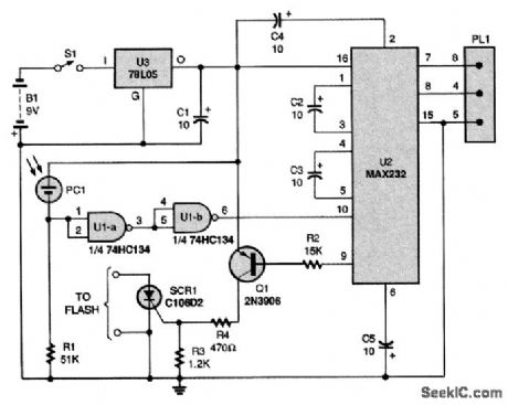
Power from a 9-V battery (B1) is fed to a 78L05 regulator (U3). The IC then produces a regulated 5 V to power the rest of the circuit. A cadmium sulfide photocell, PC1, conducts when a connected flash's ready light comes on and illuminates it. When current flows through PC1, U1-a, and U1-b, two sections of a 74HC134 quad Schmitt trigger NAND gate produce a sharp-edged TTL high. A MAX232, U2, converts the high to an RS233 low that is compatible with the PC's serial port. The MAX232 also takes an incoming serial-port pulse and converts it to TTL levels to fire the flash via SCR1, a C106D2 silicon-controlled rectifier. The circuit works with a BASIC program. That program fires the flash by sending a brief pulse through plug PL1 to the serial port's DTR pin. The program then starts timing how long it takes for the flash to recycle. In other words, the program 'looks at the CTS pin over and over until it sees that it went low. That happens when the photocell is lit by the flash's ready light. The program records the elapsed time and continues counting until 1 minute elapses. At that time, the DTR pin is cycled again to fire the flash, and the process is repeated. The test concludes when the recycle time exceeds 45 seconds. (View)
View full Circuit Diagram | Comments | Reading(1496)
100_W_LINEAR_FOR_432_MHz
Published:2009/7/14 1:46:00 Author:May

Medium-powered amplifier using 8560A conduction-cooled tetrode provides extra power needed for use of Oscar satellite in mode B on 432.15 MHz, with drive of only 7 W. Half-wave grid is fabricated from double-sided printed-circuit board. Capacitive probe to grid line serves for input coupling. Half-wave plate line is capacitively tuned by movable vanes. Article covers construction in detail.-T. McMullen, A Tramplifier for 432 MHz, QST, Jan. 1976, p 11-15. (View)
View full Circuit Diagram | Comments | Reading(814)
FREEZE_FRAME_STROBE
Published:2009/7/14 1:45:00 Author:May

A sensor input from a mike or photodetector is amplified and used to trigger an SCR, which, in turn, triggers a camera strobe. This circuit is useful for freeze-frame photos of phenomena, such as drops of water, explosions, shots, etc. (View)
View full Circuit Diagram | Comments | Reading(668)
MINI_ROULETTE
Published:2009/7/14 1:42:00 Author:May

A circuit diagram for a mini battery-powered version of roulette is shown, This circuit uses a 4017 decade counter (IC2) driving 10 LEDs. Because only one LED is ever illuminated at any one time, a common limiting resistor R4 is used. They can also be placed in alternating red/green order for added effect. The counter IC2 is clocked by IC1, a classic 555 timer connected as an astable.When the SPIN button is pressed and then released, full speed is achieved, and then the display gradually slows down until it stops on a single number. Capacitor C2 governs the oscillator speed, and resistor R3 prevents instability when the LED rotation stops. The piezo disk transducer, X1, is placed on the output of the oscillator to provide a sound effect. (View)
View full Circuit Diagram | Comments | Reading(3220)
DUAL_MODE_BATTERY_LIFE_EXTENDER
Published:2009/7/14 1:42:00 Author:May

Most voltage regulators stop functioning when the differential voltage between the input and output is reduced below a certain level. At this level, the regulator's output voltage begins to drop at an accelerated rate, resulting in a much lower voltage's being available to the circuit. To prevent this from happening, the battery voltage is monitored and a low-battery warning signal is issued, indicating the approaching end of battery life. In the circuit presented here, the voltage regulator is bypassed when a low battery level is detected-the battery is connected directly to the circuit. At high battery voltage levels, the output voltage is regulated by the linear regulator, and the low-battery indicator (LBI) comparator output is off. Also, the LB0 pin is pulled to Vbatt (input), keeping the power MOSFET off. As the input voltage drops and approaches the regulator's dropout voltage, the base current to the regulator's pass transistor reaches its maximum, turning it on very hard. Lowering the input voltage any further will result in art increase in the pass transistor's saturation voltage and a reduction in the regulator's output voltage. The input level detector's crossover voltage should be set to Vout + Vsat of the pass transistor. When the input voltage falls below the crossover point, the comparator output is turned on. This pulls the gate voltage to ground, which turns on the power MOSFET. From this point, the voltage available to the circuit is the battery voltage minus the voltage across the power FET, which is insignificant. (View)
View full Circuit Diagram | Comments | Reading(650)
4_A_FULL_WAVE_CONTROL
Published:2009/7/14 1:42:00 Author:May

When logic input to CMOS buffer goes high, load is off. Low input logic deenergizes optoisolator; clamp formed by bridge rectifier and SCR is then removed from C1, allowing it to charge through R1. When voltage across C1 reaches triggering voltage of S1 (about 8 V), MBS4992 silicon bidirectional switch fires, allowing C1 to dump charge into gate of triac. Triac and load are then turned on.R1 and C1 are chosen to give time constant small enough to fire triac early in its conduction angle (near zero crossing), to maximize load power while minimizing EMI.-A. Pshaenich, Interface Techniques Between Industrial Logic and Power Devices, Motorola, Phoenix, AZ, 1975, AN-712A, p 17. (View)
View full Circuit Diagram | Comments | Reading(736)
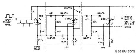
STROBOSCOPE_FLASH_UNIT
Published:2009/7/14 1:42:00 Author:May

If you retrofit a flash unit (shown in A), it can accept signals from the circuit in B to operate as a precision stroboscope (View)
View full Circuit Diagram | Comments | Reading(890)
STROBOSCOPE_TIMING_LIGHT
Published:2009/7/14 1:39:00 Author:May

The NE555 produces brief pulses of current in the wire, which is wound into a loop to increase the amount of induction. To the timing light, these pulses look like the pulses that flow through a spark-plug wire. Bear in mind that the maximum frequency of a timing light is about 20 Hz. Above that frequency, timing lights tend to skip pulses. You might be able to speed up a timing light by reducing the value of the high-voltage capacitor across the flashtube; the light will then be dimmer, but the capacitor will charge tip more quickly for the next flash. (View)
View full Circuit Diagram | Comments | Reading(5259)
175_MHz_80_W_MOBILE_FM
Published:2009/7/14 1:38:00 Author:May

Uses Motorola of transistors optimized for 12.5-V FM operation. All stages are class C. Signal-splitting techniques in input and output matching networks of power output stage minimize problems of unequal load sharing and of matching to extremely low impedance levels. Overall gain is 26 dB, and efficiency is 49.5%.-J. Hatchett, Design Techniques for an 80 Watt, 175 MHz Transmitter for 12.5 Volt Operation, Motorola, Phoenix, AZ, 1972, AN-577, p 2. (View)
View full Circuit Diagram | Comments | Reading(1667)
TRANSISTORIZED_THYRATRON_RING_COUNTER
Published:2009/7/14 1:37:00 Author:May

Each bistable circuit has two opposite-symmetry germanium transistors, two diodes, and four resistors. Additional transistor Q transfers conducting stage to next position when actuated by transfer pulse. Absence of capacitors gives high-speed operation. No bias current is required from ON stage to keep other stages cut off.-J. A. Pecar, Ring Counter Uses Transistors, Electronics, 34:4, p 49-51. (View)
View full Circuit Diagram | Comments | Reading(1218)
12_V_STROBOSCOPE
Published:2009/7/14 1:37:00 Author:May

Diode Dl is a polarity-protection device that can be omitted. A 555 is used as an astable with a frequency of about 0.7 kHz. When T1 is on, a current flows through the 6-V winding of TR1. When the collector voltage of T1 is nearly 0, the potential at the anode of D2 must be negative. When T1 becomes reverse-biased, its collector voltage rises to about 12 V and the potential at the anode of D2 must then be positive so that C4 can be charged Never operate the converter without a load. It is, perhaps, advisable to shunt C4 with a 100-kΩ, 1-W resistor. The converter charges C4 to about 300 V. This causes a potential at junction R6-05 of about 100 V. The neon lamp then comes on, so a gate current flows into the thyristor. This comes on and clears the way for C5 to discharge through TR2.This starting transformer produces a secondary voltage of a few thousand volts. This is sufficient for the xenon tube to strike and at the same time discharge C4. Then the operation can start again. The circuit draws a current of about 250 mA, but this depends on the flashing rate and the type of xenon tube. (View)
View full Circuit Diagram | Comments | Reading(1010)
40_METER_CW
Published:2009/7/14 1:37:00 Author:May

Delivers about 250 mW of RF output, operating from 6-V battery. Sidetone can be monitored with high-impedance headphones or small loudspeaker. Carrier frequency can be tuned up to 1 kHz above and below nominal frequency of 40.meter crystal-Circuits, 73 Magazine, July 1977, p 34.
(View)
View full Circuit Diagram | Comments | Reading(753)
l_KC_SCALER
Published:2009/7/14 1:37:00 Author:May

Glow-tube counter provides driving pulses of about l00 v, using two amplifiers in cascade, both saturated when no signals are present.-H. A. Kampf, Increasing Counting System Reliability, Electronics, 32:37, p 112-113. (View)
View full Circuit Diagram | Comments | Reading(558)
100_KV_FOR_ACCELERATOR
Published:2009/7/15 22:41:00 Author:Jessie
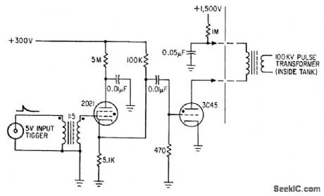
Two thyrcttrons trigger pulse amplifier to send 1,500-v pulse to primary of pulse transformer for step up to l00 kv for Van de Graaff accelerator source. -E. J. Rogers, Van de Graaff Proton Source Receives 1l0 Kilovolt Boosts, Electronics, 35:13, p 58-59. (View)
View full Circuit Diagram | Comments | Reading(1317)
| Pages:661/2234 At 20661662663664665666667668669670671672673674675676677678679680Under 20 |
Circuit Categories
power supply circuit
Amplifier Circuit
Basic Circuit
LED and Light Circuit
Sensor Circuit
Signal Processing
Electrical Equipment Circuit
Control Circuit
Remote Control Circuit
A/D-D/A Converter Circuit
Audio Circuit
Measuring and Test Circuit
Communication Circuit
Computer-Related Circuit
555 Circuit
Automotive Circuit
Repairing Circuit