
Circuit Diagram
Index 674
ONE_FILTER_THREE_PHASE_SINE_WAVE_GENERATOR
Published:2009/7/13 22:57:00 Author:May
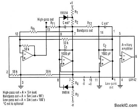


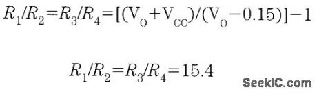


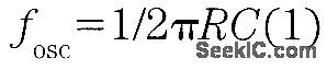

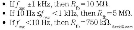


It is possible to build a three-phase sine-wave oscillator using just one UAF42 state variable filter along with some resistors and diodes. Three output nodes are available: high-pass out, bandpass out, and low-pass out. The signals at the bandpass and low-pass out nodes are 90°and 180° out of phase, respectively, with those at the high-pass out node. An on-board auxiliary op amp is available for use as a buffer or gain stage. The frequency of oscillation is set with resistors RF1 and RF2 using the simple equation:The maximumfosc obtainable using the UAF42 state-variable filter is 100 kHz. However, distortion becomes a factor for frequencies above 10 kHz. Resistance R1, R2, R3, and R4, should be selected using the following equation to set the desired signal amplitude:Resistor Rfb provides a positive feedback path from the bandpass out node to the summing-amplifier input. This provides the necessary startup required to begin oscillation. Suggested values are as follows:To design a 1-kHz,1.2-V peak oscillator,use Eq 1 to calculate RF1 and RF2∶Use Eq.2 to determine values for the signal magnitude-setting resistances R1/R2 and R3/R4:Setting R1 and R3 equal to 15.4 kΩ and R2 and R4 equal to 1 kΩ would provide the proper resistor ratios These resistors act as loads to the internal op amp (View)
View full Circuit Diagram | Comments | Reading(945)
CARBON_MIKE_FOR_MOBILE_SERVICE
Published:2009/7/13 22:53:00 Author:May


Filter enhances desirable characteristics of ordinary carbon mike taken from telephone, for use with mobile transceiver. Required excitation voltage of 3.5 V for mike is reduced from 12 V of car battery by resistor network having hash filter to keep alternator whine out of audio system. Output of 0.25 mV from mike-filter combination is reduced by 100K pot to value needed for transmitter.-S. Olberg, The Carbon Marvel, 73Mag-azine, April1977, p 120. (View)
View full Circuit Diagram | Comments | Reading(893)
500_kHz_SCAN_ON_2_METERS
Published:2009/7/13 22:52:00 Author:May
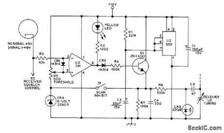
Circuit added to 2-meter transceiver sweeps 500-kHz segment of 2-meter band at 2-s intervals. When incoming signal is strong enough to trip receiver squelch, sweep stops and receiver locks on station. R4 and C3 determine scan rate. Adjust R1 for best lock-on. When signal is sensed, squelch is greater than 9 V on R3, driving output of U2 low, turning on LED, and removing charging voltage from R4. When signal disappears, output of U2 goes high and scanning continues.-W. Sward, Add Frequency Scan to a Receiver for $10, QST, March 1977, p 48. (View)
View full Circuit Diagram | Comments | Reading(1700)
7_71_MHz_VFO
Published:2009/7/13 22:51:00 Author:May

JFET Q1 serves as oscillator, with frequency determined by C2, L2, CR2, and CR3; diodes operate in reverse-bias regions as voltage-variable capacitors. Amount of reverse bias applied by R2 determines capacitance and frequency. VFO operates on both transmit and receive; on transmit, no voltage is applied to VFO offset circuit R1-C1-CR1 so it has little effect on oscillator, 0n receive, +12 V applied to R1 makes CR1 conduct and places C1 across frequency-determining network to shift VFO about 100 kHz away from operating frequency so receiver will not be blocked. Q2 is buffer between oscillator and transmitter. VR1 provides regulated 9.1 V for oscillator and buffer. (Project was named after chopped beef can in which it was mounted.)-J. Rusgrove, The CB Slider, OST, March 1977, p 15-17. (View)
View full Circuit Diagram | Comments | Reading(1169)
TEMPERATURE_COMPENSATED_LOG_CONVERTER
Published:2009/7/13 22:50:00 Author:May

Two opamps and two logging transistors give output proportional to logarithm of input with high degree of temperature compensation. Article gives design equations and application instructions. Circuit is for positive inputs; for negative inputs, use PNP transistors such as 2N4058 in place of those shown.-G. B Clayton, Experiments with Operational Amplifiers, Wireless World, Jan. 1973, p 33-35. (View)
View full Circuit Diagram | Comments | Reading(833)
SINE_WAVE_DOUBLER
Published:2009/7/13 22:50:00 Author:May


This circuit uses a four-quadrant multiplier by Analog Devices to perform frequency doubling on a sine-wave input signal. By applying a sine wave to both x and y inputs, the multiplier muitiplies the sine wave by itself, resulting in a sine-squared waveform. This waveform is equivalent to a dc level and a cosine component at twice the frequency and half the original amplitude, i.e., sin2x(1-cos 2x)/2-3 dB bandwidth is typically 30 MHz. (View)
View full Circuit Diagram | Comments | Reading(1601)
PROTECTION_AGAINST_SIMULTANEOUS_OPERATION_OF_TRIACS
Published:2009/7/13 22:48:00 Author:May

Optoisolators provide cross-connection between solid-state triac relay circuits to eliminate possibility that two or more triacs come on at same time due to circuit malfunction or component failure. Circuit shuts system down when this occurs.- Thyristor Gating for μP Applications,″ Texas Instruments, Dallas, TX, 1977,CA-191,p 5-9. (View)
View full Circuit Diagram | Comments | Reading(1675)
OUTPUT_CONTROL_FOR_CLOCK_COMPARATOR
Published:2009/7/13 22:45:00 Author:May
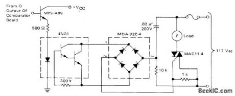
Circuit triggers 10-A triac when Q output of comparator-driven flip-flop is logic 1. LED in optoisolator is then energized, activating phototransistor pair for driving gate circuit of triac through diode bridge. Trigger voltage of triac is positive for first quadrant and negative for third quadrant, to give maximum sensitivity of triac control.-D. Aldridge and A. Mouton, Industrial Clock/Timor Featuring Back-Up Power Supply Operation,” Motorola, Phoenix, AZ, 1974, AN-718A, p 7. (View)
View full Circuit Diagram | Comments | Reading(1390)
TEMPERATURE_COMPENSATED_ANTILOG_CONVERTER
Published:2009/7/13 22:44:00 Author:May

Circuit provides antilog conversion with high degree of temperature compensation. Article gives design equations and application instructions. Circuit is for positive inputs; for negative inputs, use PNP transistors such as 2N4058 in place of those shown. Adjust value of R4 to make output of opamp A2 exactly 10 times input voltage ei when input is -1 V.-G. B. Clayton, Experiments with Operational Amplifiers, Wireless World, Jan, 1973, p 33-35. (View)
View full Circuit Diagram | Comments | Reading(1545)
SHAFT_ENCODER
Published:2009/7/13 22:44:00 Author:May

The electro-optical shaft encoder is a combination of encoding disk, photosensors, and counters. The encoding disk and photosensors generate a pulse train that can be counted to determine rate. The disk's direction of rotation can be sensed and used to determine count direction (for example, count up for clockwise and count down for counterclockwise). The disk need not be a precision part; it can be tytade from clear plastic with dark sections or lines painted on it. The number of lines on the disk determines how many pulses are generated per revolution. If two photosensors are used, two signals in quadrature are generated; from those, the direction can be sensed. A simple encoding disk is shown in A; note the alternating transparent and opaque sections. A pair of electro-optical photosensors are positioned (as shown) so that when one is centered over a section, the other is positioned over a transition. As the disk is rotated, each photosensor will be alternately illuminated and obscured and will produce outputs (as shown). A clockwise rotation is indicated when there is a positive transition (from dark section to light section) at sensor B while sensor A is low (obscured by a dark section), a positive transition at A while B is high (over a light section), a negative transition of B (going from light to dark) while A is high, and so forth. A counterclockwise rotation is indicated when there is a positive transition of B when A is high, a negative transition of A when B is high, etc. (View)
View full Circuit Diagram | Comments | Reading(2931)
ZERO_POINT_SWITCH
Published:2009/7/13 22:44:00 Author:May

Used to control resistive loads. With S1 open, triac Q2 is turned on very close to zero on initial part of positive half-cycle because of large current flow into C2.Once Q2 is on, C3 charges through D5. When line voltage goes through zero and starts negative, C3 is still discharging into gate of C2 to turn it on near zero of negative half-cycle. Load current thus flows for most of both half-cycles. When S1 is closed, Q1 is turned on and shunts gate current away from Q2 during positive half-cycles. Q2 cannot turn on during negative half-cycle because C3 cannot charge, which makes load current zero.- Circuit Applications for the Triac, Motorola, Phoenix, AZ, 1971, AN-466, p 12. (View)
View full Circuit Diagram | Comments | Reading(0)
SHAFT_ENCODER_PULSE_GENERATING_CIRCUIT
Published:2009/7/13 22:42:00 Author:May

This circuit produces one output pulse for every transition of the photosensor output or four pulses for every section or line pair. The exclusive-NOR gates U1-b and U1-c produce a pulse on every transition, and U2, a dual four-channel data selector, decodes them into up pulses or down pulses. The number of sections or lines that can be accommodated on a disk is determined by its diameter and the width of the sections. As an example, if the sections are made approximately 0.125 wide, 25 section pairs can put on a 2 diameter disk and 100 pulses will be generated with every revolution of the disk. The only limiting factor is that the sections must be wider than the photosensor's aperture at the point they pass in front of it, The alignment of the photosensor assembly is not critical. The only concern is that one sensor be over a light area while the other sensor is at a transition from light to dark or dark to light. 1Vro sections of U1, U1-a and U1-c, act as buffers and waveshapers for the outputs of the sensor, while U1-b and U1-d generate a pulse at each transistor of the sensor's output. The 100-k Ω resistors between the output and the input of U1-a and U1-c provide positive feedback to speed up the rise and fall times and also generate hysteresis to eliminate noise during the transitions. The pulses produced by U1-b and U1-d at the transitions are the result of the delay produced by the RC circuits located at one input of each gate. For example, U1-b pin 5 follows the transition immediately, whereas pin 6 follows slowly. With the values shown, the two inputs are different for about 100 μs after every transition. While the inputs are different, the output is low. Therefore, U1-b generates a negative pulse for every transition of sensor U3 and U1-d generates a negative pulse for every transition of U4. The states of U3 and U4 determine whether the pulse is sent to the X output of the data selector (U2, pin 13) to indicate a CCW pulse or to the Y output (pin 3) to indicate a CW pulse. (View)
View full Circuit Diagram | Comments | Reading(2657)
ANALOG_DIVIDER
Published:2009/7/13 22:39:00 Author:May

Optical Electronics 2457 logarithmic module containing two pair of bipolar log elements and three opamps drives single 395 opamp to provide analog division function with high accuracy and wide dynamic range. Input resistors set full-scale input voltage. R3 determines AC accuracy. Connect inputs together fot drive with signal varying between 100 mV and 10 V (1% to 100%of full scale), and adjust R3 for straight-ine output at1 V. For negative inputs, reverse diode connections and make reference voltage negative.- Accurate Logarithmic Analog Divider, Optical Electronics, Tucson, AZ, Application Tip 10213. (View)
View full Circuit Diagram | Comments | Reading(2144)
BATTERY_CHARGER
Published:2009/7/13 22:39:00 Author:May

This current-source battery charger can source 2.5 A with up to 96 percent efficiency. It can operate from an ac adapter or directly from a car battery. By sensing current on the high side of the battery being charged, it preserves the low impedance of the automobile's ground-return system. The charger handles battery stacks of 5 to 15 cells, and its input voltage can range from 28 V down to a level 1.5 V above the terminal voltage of a fully charged battery. Charging current is generated by the current-mode, buck-regulator controller IC1, operating with an external power switch (Q1) and a synchronous rectifier (Q2). Both are N-channel MOSFETs, whose low on-resistance (vs. P-channel types) contributes to high efficiency in the circuit. The IC includes a charge pump for generating the required positive gate voltage for Q1. It also senses the Q1 current (via R1) and shuts down if this current becomes excessive.The current-sense transformer (T1) saves power by diverting a fraction of Q1's current through R1. Operating on the output's high side is the current-sense amplifier IC2. Its OUT current (1/2000 of the current flowing internally from RS+ to RS-) flows through R2 to produce a feedback signal for IC1. Digital control of the charging current can be introduced by switching among different-switching FETs like the 2N7002; its 7.5-Ω on-resistance is not a problem because its drain current-no greater than 1.25 mA-introduces an error no greater than 0.5 percent. Circuit efficiency ranges up to 96 percent. Efficiency and power output both increase with output voltage, because the circuit's power consumption (associated mainly with IC1 and the switching MOSFETs) is almost constant. This buck regulator's output cannot rise about Vin in most cases, overvoltage protection is not required. VOUT which supplies power to IC2, must not go below 4 V. (View)
View full Circuit Diagram | Comments | Reading(0)
OPTOISOLATOR_DRIVE
Published:2009/7/13 22:35:00 Author:May

TL440 zero-crossover switch uses pulsed gate drive. Switch supplies phase-locked driving pulses during zero-voltage crossover period, to minimize electromagnetic interference generated during turn-on of triac. Works well with resistive loads, but inductive loads can create phase shift that affects firing time of triac.- Thyristor Gating for μP Applications, Texas Instruments, Dallas, TX,1977,CA-191,p 6. (View)
View full Circuit Diagram | Comments | Reading(2062)
LOGAMP_TESTER
Published:2009/7/13 22:34:00 Author:May
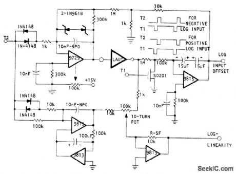
Circuit sweeps logamp under test (LAUT) over its dynamic range while automatically canceling offset voltage at input, with output serving as indication of this offset voltage. Exponential deeay voltage generated is accurate from 10 V to 100 μV. At time zero, pulse T2 is applied to Optical Electronics 9729 opamp connected as exponential generator, charging NPO feedback capacitor to 10V. At end of pulse, opamp output voltage decays exponentially. Input pulse also generates ±10 V precision reference ramp in pair of 9813 opamps. Output of LAUT is compared with reference ramp; any difference is proportional to nonlinearity of logamp.- Testing Logarithmic Amplifiers, Optical Electronics, Tucson, AZ, Tech Tip 10268. (View)
View full Circuit Diagram | Comments | Reading(711)
SEISMIC_RADIO_BEACONRF_POWER_AMPLIFIER
Published:2009/7/13 22:32:00 Author:May

This RF power amplifier operates at 432 MHz and was used as a power amplifier for a small transmitter used in an amateur radio beacon that also has seismic monitoring capability. (View)
View full Circuit Diagram | Comments | Reading(876)
TTL_INTERFACE_FOR_VMOS
Published:2009/7/13 22:32:00 Author:May

By using opencollector 7416 TTL interface with its output pulled up to 15V,S55V01 VMOS will switch up to 2 A easily. Inductive load such as relay requires diode across relay coil-L. Shaeffer, VMOS Peripheral Drivers Solve High Power Load Interface Problems, Computer Design,Dec.1977,p 90,94,and 96-98.
(View)
View full Circuit Diagram | Comments | Reading(650)
90_PERCENT_EFFICIENT_FOUR_CELL_NiCd_CHARGER
Published:2009/7/13 22:31:00 Author:May

An embedded battery charger requires extremely low power dissipation in order to minimize heat buildup in compact portable systems. This schematic shows a charger that can charge four NiCd cells and is selectable for either a 1.3-A fast charge or a 100-mA trickle charge with up to 90 percent efficiency. The LTC1148 is a step-down synchronous switching regulator; it controls the charge rate, monitoring the output current via external current-sense resistor R3. Fast charge current is determined by the value of R3, according to the fast charge equation. In this case, it is set to 1.3 A. The resistor divider network R4 and R5 sets the output voltage to a nominal 8.1V under noload conditions, such as when the battery is removed. A four-cell NiCd pack's voltage will range from 3.6 to 6 V, depending upon its state of charge. When installed, the battery will pull the output below 8.1 V and place the LTC1148 into current-limited operation at 1.3 A. This constant current will be delivered until trickle charge is enabled by an external charge termination circuit or the battery is removed. Q3 enables trickle charge operation with charge current set by choice of R1. Diode D2 prevents the battery from being drained by the feedback resistor network when the LTC1148 is shut down.
(View)
View full Circuit Diagram | Comments | Reading(924)
WARM_UP_DRIFT_COMPENSATOR
Published:2009/7/13 22:30:00 Author:May

Warm-up drift of transceiver VFO is automatically corrected by using binary counter U1 to count oscillator frequency for interval of about 3.81 Hz determined by 1-MHz reference crystal oscillator and divider chain U4-U5. Switches labeled UP and D0WN are used to bring output of integrator R3-C3 into range manually after circuit switch-on. –K. Spaargaren, Drift-Correction Circuit for Free-Running Oscillators, Ham Radio, Dec, 1977,, p 45-47. (View)
View full Circuit Diagram | Comments | Reading(666)
| Pages:674/2234 At 20661662663664665666667668669670671672673674675676677678679680Under 20 |
Circuit Categories
power supply circuit
Amplifier Circuit
Basic Circuit
LED and Light Circuit
Sensor Circuit
Signal Processing
Electrical Equipment Circuit
Control Circuit
Remote Control Circuit
A/D-D/A Converter Circuit
Audio Circuit
Measuring and Test Circuit
Communication Circuit
Computer-Related Circuit
555 Circuit
Automotive Circuit
Repairing Circuit