
Circuit Diagram
Index 662
ELECTRONIC_TURBIDIMETER
Published:2009/7/15 22:40:00 Author:Jessie

A turbidimeter is a scientific instrument used to measure the cloudiness of solutions,such as water,if you measure the amount of scattered light,you can measure the turbidity. Paint the inside of the test-tube holder flat black Glue a cadmium sulfide photoresistor (R2)to a cardboard disk,and glue the assembly to the open end of the 90°tube Next,cement a biconvex lens (one that curves outward on both sides) to the bottom of the test-tube holder. Power up I1,a 12-V, 1-A automotive light bulb, and hold it at various distances below the biconvex lens. Find the distance at which a beam of light comes straight up the tube or converges slightly, but does not diverge. Mount the lamp and play it on the 100-μA meter; the resistors on the rotary switch set the sensitivity or attenuation. Power is supplied to the circuit by two 9-V batteries in a split supply; I run the lamp off a separate 12-V supply. If you want truly calibrated readings, you'll need to buy a turbidity standard solution, available in JTU (Jackson Turbidity Units) and NTU (Nephelos Turbidity Units), from a science-sup-ply company. In operation, zero the meter to a clean-water blank, note the reading from a known standard, note the reading from the unknown sample, and calculate the sample's turbidity, based on the needle's position. (View)
View full Circuit Diagram | Comments | Reading(2538)
ZERO_CROSSING_CONTROL
Published:2009/7/14 1:37:00 Author:May

When control signal calls for power, optoisolator energizes circuit that provides load turn-on at zero-voltage time of AC waveform. If phototransistor Q3 of optoisolator is illuminated after S1 drops to 1-V conduction voltage of MUS4988, triacs will not be turned on. Circuit thus provides relay-enabling voltage window, lower limit of which is point at which all components involved in turning on triacs are forward-biased. Upper limit is nominal 8-V breakover voltage of unilateral switch S1. S2 performs similar function on negative voltage alternations. Load-controlling triac is rated 40 A.-T. Mazur, Solid-State Relays Offer New Solutions to Many Old Problems, EDN Magazine, Nov. 20, 1973, p 26-32. (View)
View full Circuit Diagram | Comments | Reading(1260)
SYNC_FOR_SCR_PARALLEL_INVERTER
Published:2009/7/15 22:40:00 Author:Jessie

Double-output pulse generator uses two relaxation oscillators synchronized by C3 to produce high-energy pulses alternately from two separate sources, in correct timing sequence from instant that supply voltage is switched on. Synchronism is required to prevent inverter failure.-SCR Parallel Inverters in Correct Timing Sequence, Electronic Circuit Design Handbook, Mactier Pub. Corp., N.Y., 1965, p 66. (View)
View full Circuit Diagram | Comments | Reading(1332)
HEADS_OR_TAILS_GAME_CIRCUIT
Published:2009/7/14 1:35:00 Author:May

Designed to simulate by electronic means thetossing of a coin,the circuit is based upon a 4049 hex inverter IC, two of which are used. IC1a andIC1b are wired as an astable oscillator, which causes two LEDs(D1 and D2) to alternate rapidly,at a frequency too high to be distinguished by thenaked eye. Both LEDs, therefore, appear to be constantly illuminated. when the SPIN switch S2 is closed, this has the effect of freezing the display,and the LED, which was illuminated at the instantthat the switch was closed, will now be continuously alight. Opening the switch enables the oscillator once more . There is an equal chance of either LED lighting,and the circuit can be used in boardgames, for example, to choose which player will move first. (View)
View full Circuit Diagram | Comments | Reading(808)
TWO_AMPLIFIERS_FOR_BIPOLAR_PULSES
Published:2009/7/15 22:38:00 Author:Jessie

Design procedure is based on fact that wide bandwidth is required only for leading and trailing edges of pulses. Auxiliary amplifier supplies current to charge load and stray capacitances, reducing standby current and improving gain. Auxiliary amplifier V4.VS provides charging current for shunt capacitance during positive-going edge of output pulse.-J. F. Golding, Novel Approach to Pulse Amplifier Design, Electronics, 33:1, p 64-66. (View)
View full Circuit Diagram | Comments | Reading(546)
WRONG_POLARITY_PROTECTION
Published:2009/7/15 22:38:00 Author:Jessie

Provides built-in protection of transistors in inverter from incorrect polarity of connection to 12-v battery. Used between inverter and battery. Green bulb G lights and relay operates for correct polarity. With wrong polarity, relay does not operate and red bulb R comes on to indicate error.-J. J. Pirch, Inverter Control, EEE, 11:3, p 44. (View)
View full Circuit Diagram | Comments | Reading(703)
RING_COIJNTER_WITH_VISUAL_READOUT
Published:2009/7/14 1:35:00 Author:May

Uses only six components per stage. Combining of counter and indicator functions gives low battery drain. After reset button is re leased, 0.22-mid capacitor insures that first stage turns on. Current is drown by stage only when lamp is on. Any number of stages may be included in ring.- Transistor Manual, Seventh Edition, General Electric Co., 1964, p 203. (View)
View full Circuit Diagram | Comments | Reading(585)
SELF_EXCITED_HALF_BRIDGE
Published:2009/7/15 22:37:00 Author:Jessie

Uses only two transistors. Suitable for both two-phase and three-phase applications. Basic circuits can be connected in series for high-voltage operation. Maximum transistor off voltage equals input voltage of half-bridge, making 80-v inverter practical for germanium transistors and 150 v for silicon.-A. G. Lloyd, Half-Bridge Inverter Provides Economical Three. Phase Power, Electronics, 34137, p 62-65. (View)
View full Circuit Diagram | Comments | Reading(2029)
LOGIC_DRIVES_TRIAC
Published:2009/7/14 1:33:00 Author:May

H74C1 optoisolator combined with saturation characteristic of ordinary filament transformer serves to trigger full-wave triac on or off under control of logic input, for energizing AC loads up to rating of triac. Logic 0 (ground level) turns load on, and logic 1 turns it off.-D. D. Mickle, Practical Computer Projects, 73 Magazine, Jan. 1978, p 92-93. (View)
View full Circuit Diagram | Comments | Reading(723)
LOCKOUT_CIRCUIT_
Published:2009/7/14 1:33:00 Author:May

This circuit is used in contests,games,etc When a contestant presses one of the buttons,an SCR triggers,lighting the associated LED and preventing anyone else from actuating the system .U2 and U3 form a warble tone generator, while U4 and U5 provide time delay. (View)
View full Circuit Diagram | Comments | Reading(1820)
WIDEBAND_DIGITAL_PULSE_AMPLIFIER
Published:2009/7/15 22:37:00 Author:Jessie

Common-emitter ac coupled cascaded amplifiers, with negative feedback at every second stage, give voltage gain of 12, bandwidth of 100 Mc, rise time of 3 nsec, pulse pair resolution of 5 nsec, and s/n ratio of 100 to1 for inputs from 0 to 200 my.-A. A. Fleischer and E. Johnson, New Digital Conversion Method Provides Nanosecond Resolution, Electronics, 36:18, p 55-57. (View)
View full Circuit Diagram | Comments | Reading(924)
POSITIVE_FEEDBACK_BOOSTS_SWITCHING_SPEED
Published:2009/7/15 22:36:00 Author:Jessie

Base resistors R1 and R2 allow addition of cross-coupled positive-feedback capacitors C1 and C2 to increase high-frequency gain of feedback loop and provide energy storage to drive oaf transistor fully on when core saturates.-A. G. Lloyd, Speed-Up Circuits Improve Switching of Transistor Inverters, Electronics, 34:45, p 92-94. (View)
View full Circuit Diagram | Comments | Reading(567)
LOGIC_DRIVES_SCR_
Published:2009/7/14 1:32:00 Author:May

Uses light-activated SCR in H74C1 optoisolator to trigger larger SCR for controlling loads up to 3000 W through bridge diodes, When logic input goes low (to ground), load is energized. Limit for inductive loads is 8 A or about 1000 W if using 25-A SCR.-D. D.Mickle, Practical Computer Projects, 73 Magazine, Jan. 1978, p 92-93. (View)
View full Circuit Diagram | Comments | Reading(909)
VOICE_EFFECTS_SIMULATOR_CIRCUIT
Published:2009/7/14 1:31:00 Author:May

The circuit design shown produces a Dr Who Dalek voice effect by chopping an audio signal at a low frequency. The best frequency seems to be around 50 to 90 Hz, and this is generated by IC1, a 555 timer. The arrangement shown is not an ordinary 555 astable multivibrator, but a hysteresis oscillator, which frees the 555 internal discharge transistor (pin 7) to act as a chopper, shunting the signal to 0 V internally. The chopped frequency is set by VR1, which is adjusted to give the most realistic sound. The input signal should be in the region of 50 to 150 mV rms from a low-impedance source-e.g., possibly a dynamic microphone-to avoid clipping the signal. The diode D1 is optional, and prevents the signal from losing symmetry, if overdriven. The output signal is fed to an external amplifier. The two dc-blocking capacitors C1 and C2 are optional and are needed only if any dc bias is present on the input signal side. (View)
View full Circuit Diagram | Comments | Reading(2361)
400_CPS_FORK_CONTROL
Published:2009/7/15 22:35:00 Author:Jessie

Tuning-fork oscillator gives frequency accuracy of 0.01% for d-c to a-c inverter. Consists essentially of two-stage amplifier, output of which is regeneratively coupled to input through tuning fork.-R. Wileman, Linear Circuits Regulate Solid-State Inverter, Electronics, 33:16, p 61-63. (View)
View full Circuit Diagram | Comments | Reading(850)
ANODE_TRIGGERED_RING_COUNTER
Published:2009/7/14 1:29:00 Author:May

Triggered by coupling emitters of transistors Q1 to common bus, to permit both forward and reverse operation. Use of pnp-npn pairs reduces power requirements, improves load capacity, increases speed, and simplifiers circuits.-N. C. Hekimian, PNP-NPN CIRCUITS: New Look at a Familiar Connection, Electronics, 35.47, p 42-46. (View)
View full Circuit Diagram | Comments | Reading(1684)
PARALLEL_SQUARE_WAVE_D_C_TO_A_C_INVERTER
Published:2009/7/15 22:33:00 Author:Jessie

Receives square-wave inputs from separate drive circuit (not shown), causing Q1 to conduct half the time while Q2 is blocking, and vice-versa. Current from 28-v supply flows alternately through halves of transformer primary, to produce 400-cps a-c voltage across load.- Transistor Manual, Seventh Edition, General Electric Co., 1964, p 235. (View)
View full Circuit Diagram | Comments | Reading(630)
BACKWARD_OR_FORWARD_COUNTER
Published:2009/7/14 1:28:00 Author:May
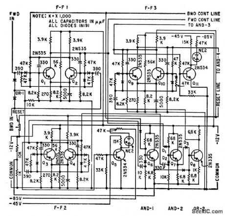
Adds or subtracts pulses under control of appropriate logic circuits. All flip-flops are identical, operating in saturation mode for maximum stability.-H.J.Weber, Binary Circuits Count Backwards or Forwards, Electronics, 32:39, p 82-83. (View)
View full Circuit Diagram | Comments | Reading(675)
PROGRAMMABLE_CONTROLLER_LIGHT_SENSOR_INTERFACE
Published:2009/7/15 22:32:00 Author:Jessie

As long as an object remains between LED1 and Q1, no output occurs. But as soon as the object moves out from between the LED and the phototransistor, IC1 (a 555 timer) is triggered, producing a timed output pulse. This circuit can be used to indicate when a part has moved away from a location. (View)
View full Circuit Diagram | Comments | Reading(794)
450_470_MHz_AT_25_W
Published:2009/7/14 1:27:00 Author:May

Power amplifier for land-mobile 12.5-V transmitter is constructed on double-sided microstrip substrate. Power gain at 470 MHz is 19.5 dB, and overall efficiency is 47%.-G. Young, UHF Microstrip Amplifiers Utilizing G-10 Epoxy-Glass Laminate, Motorola, Phoenix, AZ, 1976,AN-578, p 4. (View)
View full Circuit Diagram | Comments | Reading(520)
| Pages:662/2234 At 20661662663664665666667668669670671672673674675676677678679680Under 20 |
Circuit Categories
power supply circuit
Amplifier Circuit
Basic Circuit
LED and Light Circuit
Sensor Circuit
Signal Processing
Electrical Equipment Circuit
Control Circuit
Remote Control Circuit
A/D-D/A Converter Circuit
Audio Circuit
Measuring and Test Circuit
Communication Circuit
Computer-Related Circuit
555 Circuit
Automotive Circuit
Repairing Circuit