
Circuit Diagram
Index 667
LIN_LOG_SWEEP
Published:2009/7/14 0:30:00 Author:May

Sweep rate and center frequency are adjustable in versatile sweep generator providing sweep-frequency output and both linear and logarithmic voltages representing output frequency. Optical Electronics 3329 voltage-to-frequency transducer generates sweep voltage at frequency determined by external resistors, capacitor, and input voltage from 10K pot. Sweep waveform is triangular; for sawtooth waveform, change one of 100K timing resistors to 10K. Second 3329 delivers frequency-varying sine wave to 9110B buffer. 10K pot determines center frequency. Stable log f output is obtained with 2457 log module, Frequency and sweep rates can be range-switched from DC to 100 kHz by changing timing capacitor.- Improved Sweep Generator, Optical Electronics, Tucson, AZ, Application Tip 10209. (View)
View full Circuit Diagram | Comments | Reading(2308)
LEAD_ACID_BATTERY_TEMPERATURE_COMPENSATED_CHARGER
Published:2009/7/14 0:27:00 Author:May

The charging characteristics of lead-acid cells are strongly linked to the ambient temperature. To prevent over-or undercharging of the battery during periods of extended low or high temperatures, temperature compensation is desirable. This circuit incorporates a low-dropout linear regulator, temperature compensation, dual-rate charging, and true negative ground, and consumes zero standby current. The LT1086 linear regulator is used to control the charging voltage and limit maxi-mum charging current. If the input supply is removed, Q1 and Q2 turn off and all charger current paths from the battery to ground are interrupted, resulting in zero shutdown current draw. Diode D1 provides reverse current flow protection for the regulator should the input fall below the battery voltage or be shorted. The temperature compensation employed in this circuit follows the true cur-vature of a lead-acid cell. Temperature compensation is provided by RTH, which is a Tempsistor, in parallel with R3. Changes in temperature alter the resistor divider ratio of the regulator. The match is within 100 mV for a 12-V battery over a range of -10 to +60℃. The best location for the Tempsistor is directly under the battery, with the battery resting on a pad of Styrofoam. Dual-rate charging is implemented by comparator LT1012, which senses the charging current through current-sense resistor RS. When the current is greater than 10 mV/RS, the high-rate charging voltage is 14.4 V at 25℃; when the current is less than this threshold, the float charging voltage is 13.8 V. (View)
View full Circuit Diagram | Comments | Reading(1907)
FEEDBACK_CONTROL
Published:2009/7/14 0:22:00 Author:May

Replacement of manual phase control pot with sensor and transistor provides automatic control of load power in response to stimuli such as heat, light, pressure, or magnetic fields. Output of feedback control circuit goes to thyristor in series with load. RC establishes desired operating point for sensing resistor RS. As RS increases in resistance, more current flows into CT and makes 2N4870 UJT trigger at smaller phase angle so more power is applied to load. For opposite effect, interchange RS and RC.-D. A. Zinder, Unijunction Trigger Circuits for Gated Thyristors, Motorola, Phoenix, AZ, 1974, AN-413, p 4. (View)
View full Circuit Diagram | Comments | Reading(809)
SIMPLE_CHARGER
Published:2009/7/14 0:11:00 Author:May

Built with just four components, this battery charger for small NiCd batteries is useful as a compact travel charger or in floating simple battery-backed projects. It is small enough to fit in a 35-mm film canister.Warning: This circuit is not isolctted from the ac line cmd presents a shock hazard if there is any contact between it and a person or another device. (View)
View full Circuit Diagram | Comments | Reading(871)
FLOAT_CHARGING_CIRCUIT
Published:2009/7/14 0:05:00 Author:May

To float-charge a 12-V lead-acid battery, all you need is an accurately regulated 13.8-Vdc power supply. You could connect the power supply directly to the battery, but it is safer to make the connection through a couple of 12-V, 1-A automotive light bulbs. The light bulbs serve as current limiters; they guarantee that no matter what happens, the power supply will never have to deliver more than 2 A. Resistors can also serve as current limiters, but light bulbs are better because their resistance varies with current in a useful way. It's nearly zero at low current, but as the current through each bulb approaches 1 A the bulb lights and the resistance increases. Thus, the bulb limits the current, but doesn't waste energy when the current is low. This setup is a good way to power a heavy load that operates intermittently, such as a ham radio transmitter. The battery delivers heavy current when necessary and the power supply keeps the battery charged. (View)
View full Circuit Diagram | Comments | Reading(815)
FREQUENCY_SYNTHESIZER_
Published:2009/7/13 23:55:00 Author:May

The MAX038 and four other ICs can form a crystal-controlled, digitally programmed frequency synthesizer that produces accurate sine, square, or triangle waves in 1-kHz increments over the range 8 kHz to 16.383 MHz. Each of the 14 manual switches (when open) makes the listed contribution to output frequency: Opening only S0, S1, and S8, for example, produces an output of 259 kHz. The switches generate a 14-bit digital word that is applied in parallel to the D/A converter (IC2) and a ÷N circuit in IC1. IC1 also includes a crystal-controlled oscillator and high-speed phase detector, which form a phase-locked loop with the voltage-controlled oscillator in IC5. The DAC and dual op amp (IC4) produce a 2- to 750-μA current that forces a coarse setting of the IC5 output frequency-sufficient to bring it within capture range of the PLL. This loop, in which the phase detector in IC1 compares IC5's SYNC output with the crystal-oscillator frequency divided by N, produces differential-phase information at PDV and PDR. IC3 then filters and converts this information to a ±2.5-V single-ended signal, which, when summed with an offset and applied to FADJ, forces the signal output frequency to the exact value set by the switches. (View)
View full Circuit Diagram | Comments | Reading(1778)
ZERO_SET_FOR_90_DIODE_MATRIX
Published:2009/7/13 23:49:00 Author:May

Each pulse input to lip-lop advances counter one position. Single-transistor amplifiers A1-A0 drive glow indicator tube serving as readout. For reset to zero, positive pulse is applied to base of transistor in zero amplifier, to turn its transistor on and turn all other amplifier transistors off.-R.W. Wolfe, Diode Matrix Shrinks Decimal Counter, Electronics.35:13,P50-52 (View)
View full Circuit Diagram | Comments | Reading(555)
RING_OF_7_COUNTER
Published:2009/7/13 23:48:00 Author:May
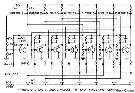
Uses surface-barrier transistors in arrangement wherein pattern of four on stages is stepped along ring, per mining maximum number of stages in ring lo be much higher than in conventional rings.-W. Carlson, Ring Counter has Increased Count Capacity, Electronis 31:15, p 89-91. (View)
View full Circuit Diagram | Comments | Reading(1462)
COMMAND_TIME_COUNTER
Published:2009/7/13 23:46:00 Author:May
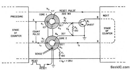
Used with time-logic matrix to store command times for missile-launching and guidance-control systems.-W.R. Johnston, Multiaperture-Core Counters Give Nondestructive Storage Readout, Electronics, 34:24, p 62-64. (View)
View full Circuit Diagram | Comments | Reading(786)
CONSTANT_CURRENT_NiCd_CHARGER
Published:2009/7/13 23:46:00 Author:May

A tapped transformer(T1)with two rectifier diodes (D1 and D2) and capacitor C1 provides the primary dc supply from the 230 Vac The power MOSFET device TR3 is initially biased into conduction by a positive gate voltage from resistor R3 Current flowing through the load flows through Current-sensing resistor R4,developing a voltage When this reaches about 0.5 V, transistor TR2 begins to conduct,reducing the gate (g) voltage of TR3 The circuit stabilizes at the load current that gives 0.5 V across R4 Zener diode D4 prevents excessive gate voltage from being applied to power MOSFET TR3,which might happen if the circuit was powered without the load connected,Diode D6 compensates for the base-emitter voltage drop of transistor TR1 so that the voltage across R4 is duplicated across resistor R1,controlling the current flow through LED D3 The apparent brightness of LED D3 therefore depends on the charging current,so any problems with connection to the cells on charge will be immediately apparent to the user Diode D5 prevents any “back feeding” of current from the batteries power supply fails while the batteries are still connected (View)
View full Circuit Diagram | Comments | Reading(2513)
SOUND_OPERATED_SWITCH
Published:2009/7/13 23:46:00 Author:May

An electret microphone is placed directly in front of the scanner speaker. When the microphone (X1) picks up sound (usually voice) from the speaker, the sound signal is amplified and detected, activates a retriggerable one-shot circuit, and controls the relay (K1). The relay controls the AM radio speaker, muting it when sound is detected from the scanner. (View)
View full Circuit Diagram | Comments | Reading(0)
MARKER_GENERATOR
Published:2009/7/13 23:45:00 Author:May
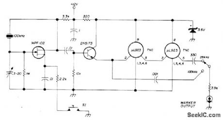
Crystal-controlled frequency marker for 80-meter SSB transceiver provides front-panel control of either 25-or 100-kHz markers. S1 activates circuit by completing source circuit of FET momentarily. Two μL923 JK flip-flops divide 100-kHz crystal frequency Down to 25 kHz 3-20 pF trimmer is adjusted to zero-beat crystal against receiver tuned to WWW.-D Hembling, Solid-State 80-Meter SSB Transceiver, Ham Radio, March 1973, p 6-17. (View)
View full Circuit Diagram | Comments | Reading(0)
SLOT_FILTER
Published:2009/7/16 1:45:00 Author:Jessie

Interval-sensitive gate will detect tone in range from 4,900 to 5,100 cps regardless of other frequencies present.-A. Corbin, Digital Tone Filter with Infinite Rejection Slope, Electronics, 34:5, p 58. (View)
View full Circuit Diagram | Comments | Reading(613)
1_A_12_V_REGULATED_SUPPLY
Published:2009/7/16 1:44:00 Author:Jessie

Using a junked VCR power transformer, this circuit supplies 12 V at 1 A. (View)
View full Circuit Diagram | Comments | Reading(645)
PUMPED_TUNNEL_DIODE_TRANSISTOR_LOGIC_GATE
Published:2009/7/16 1:43:00 Author:Jessie

Nipo gate accepts negative inputs and provides positive outputs, while pino gate accepts positive inputs and provides negative outputs. With no inputs, 200-Mc pump or dock has sufficient amplitude to fire nipo stage tunnel-diode on positive half-cycle and pino stage tunnel-diode on negative half-cycle. When input signal is present, pump cannot ire that tunnel diode; this is basic nor gate action, with output pulse only when there is no input.-E. Gottlieb and J. Giorgis, Tunnel-Diode Switching Circuits, Electron'nos, 36:27, p. 26-31. (View)
View full Circuit Diagram | Comments | Reading(664)
RF_SENSING_TB_SWITCH
Published:2009/7/13 23:43:00 Author:May

System detects presence of RF at output of transmitter and changes antenna connection from receiver to transmitter instantly and automatically. No modifications are required for transmitter or receiver. RF voltage divider R1 permits use with transmitters of any power. Broadband amplifier Q1 feeds voltage doubler CRl-CR2 through broadband toroidal step-down transformer T1.CR6, R7, and R6 form adjustable timing network that governs hold-in time of relay K1. Inverting amplifier U1 turns on Q2 for energizing K1 and switching antenna to transmitter when RF is sensed. When no rectified RF reaches UI, Q2 is cut off and antenna is changed over to receiver. RFC1 and BFC2 have 42 turns No. 28 enamel on Amidon FT-50-43 core, T1 uses Amidon FT-50-43 core, with 25turns No. 28 enamel for primary and 5 turns No. 28 over this for secondary.-D. DeMaw and J. Rusgrove, An RF-Sensed Antenna Changeover Relay, 0ST, Aug. 1976, p 21-23. (View)
View full Circuit Diagram | Comments | Reading(1441)
NEON_PHOTOCONDUCTOR_IN_LOW_COST_LOW_SPEED_GATE
Published:2009/7/16 1:43:00 Author:Jessie

Cadmium selenide or cadmium sulfide photoconductors PC deposited on common substrate are used in pairs with Ne-2H miniature neon indicator lamps to replace electromechanical relays in low-speed digital gate. Firing time of neons is reduced and stabilized by applying 350 V, 60-cps voltage between one neon electrode and adjacent external electrode, to maintain am bient light that gives low level of ionization in lamp.-J. L. Patterson, Will Neon Photo-conductors Replace Relays in Low-Speed Logic?, Electronics, 36:18 p 46-49. (View)
View full Circuit Diagram | Comments | Reading(596)
MELODY_SOUND_TO_LIGHT_CIRCUIT
Published:2009/7/13 23:43:00 Author:May

A method of synchronizing a simple light show to a musical chip is given by the circuit diagrant shown. Here, a display of eight rows of four LEDs advances with each musical note. IC2 is a UM66 three-pin melody chip selected to generate the desired tune.When power is applied to IC2, the sequence plays once and then stops. Power must be reapplied to initiate a further rendition.IC1 is a 555 astable, which will constantly reenable the tune chip and repeat the melody. However, the maximum supply voltage of the UM66 range is 3.3 V; hence, a simple zener-diode supply based around two 500-mW 2V7 types (D1 and D2) is used. TR1 is a directly driven transistor amplifier and the melody is played through loudspeaker LS1. Each musical note, when present, also biases transistor TR2 on, which shunts capacitor C2 to ground. In the absence of a note, C2 charges, which causes op amp IC3 to change state at a point determined by preset potentiometer VR1. The output from IC3, pin 6, provides a clock pulse for IC4, a 4022 divide-by-8 counter. Its outputs drive a buffer transistor sequentially to illuminate a series of four LEDs. The light display then advances with each note. (View)
View full Circuit Diagram | Comments | Reading(1667)
STEPPING_SWITCH_POSITION_INDICATOR
Published:2009/7/16 1:43:00 Author:Jessie

Transistor Q generates positive output pulse when input pulse is applied or removed. To obtain such positive pulses when stepping switch of automatic test set reaches positions 1, 3, 4, 5, 8, and 10, contacts ore connected to -10 V. Transfer for contact 1 to 2 then gives no output pulse, but moving from 2 to 3 removes input pulse and thus gives deisired output pulse. Operation depends on under clamped oscillation in unloaded R-L-C ' circuit, with only one negative oscillation because saturated transistor shunts tuned network.-R. J. Bouchard, Positive. Pulse Gen. orator, Electronics, 37:21, p 74-75. (View)
View full Circuit Diagram | Comments | Reading(675)
UP_OR_DOWN
Published:2009/7/13 23:40:00 Author:May

Scr ring counter shifts up or sown in 3 millisec without missing count. Only conducting stage draws power.-J.G. Peddie, SCR Ring Counter Switches Up or Down. Electronics.38:18.p84-85 (View)
View full Circuit Diagram | Comments | Reading(986)
| Pages:667/2234 At 20661662663664665666667668669670671672673674675676677678679680Under 20 |
Circuit Categories
power supply circuit
Amplifier Circuit
Basic Circuit
LED and Light Circuit
Sensor Circuit
Signal Processing
Electrical Equipment Circuit
Control Circuit
Remote Control Circuit
A/D-D/A Converter Circuit
Audio Circuit
Measuring and Test Circuit
Communication Circuit
Computer-Related Circuit
555 Circuit
Automotive Circuit
Repairing Circuit