
Circuit Diagram
Index 675
SEISMIC_RADIO_BEACON(TIMER_AND_SWITCHING)
Published:2009/7/13 22:30:00 Author:May

This timing circuit is fed by a threshold circuit that is actuated by selsmlc activity, as picked up by a geophone The timing is adjustable and controls a 123-Hz PL tone that feeds a transmitter (View)
View full Circuit Diagram | Comments | Reading(620)
POWER_OPAMP_FOR_CONTROL
Published:2009/7/13 22:29:00 Author:May
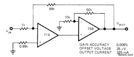
Precision 714 opamp drives 759 power opamp to give ultraprecision power amplifier system. High current capability (up to 500-mA peak output current) makes circuit suitable for such control applications as driving motors, relays, solenoids, or transmission lines. Article tells how to calculate heatsink requirements for opamp.-R. J. Apfel, Power Op Amps-Their Innovative Circuits and Packaging Provide Designers with More Options, EDN Magazine, Sept. 5, 1977, p 141-144. (View)
View full Circuit Diagram | Comments | Reading(1536)
TR_SWITCH
Published:2009/7/13 22:28:00 Author:May

Consists of driver transistors Q1 and Q2 and reed relays K1-K3. K1 switches antenna from receiver to transmitter, K2 grounds receiver input, and K3 keys transmitter. Coil of K1 has 400 turns No. 32 enamel, while K2 and K3 each have 120 tums. Coils are wound directly on glass of reed relays and covered with epoxy cement. LED normally glows dimly, with brightness increasing when character is keyed.-J. H. Fox, An Integrated Keyer/TR Switch, QST, Jan. 1975, p 15-20. (View)
View full Circuit Diagram | Comments | Reading(1396)
TRANSMIT_MIXER
Published:2009/7/13 22:28:00 Author:May
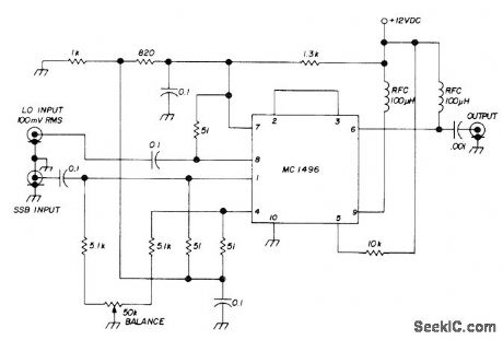
Used in low-power transceiver for 20-meter amateur band. VFO input, tunable from 5 to 5.55 MHz, is combined with 9-MHz output of crystal oscillator in Motorola MC1496G double-balanced modulator to give 14-MHz output for transmitter power chain. Supply voltage (+12 V) is applied only when transmitting. Transformers are wound on Amidon T-50-6 toroids or equivalent. Balance is Balance is maintained in mixer with center-tapped tuned circuit in output, made by putting 15-turn bifilar winding on toroid core and tuning series combination. Article gives all other circuits of transceiver.-W. Hayward, Low-Power Single-Band CW Transceiver, Ham Radio, Nov. 1974, p 8- 1 7. (View)
View full Circuit Diagram | Comments | Reading(2358)
HALF_WAVE_FEEDBACK
Published:2009/7/13 22:27:00 Author:May

Provides phase control of power to resistive load in applications where average load voltage is desired feedback variable. RC network R1-R2-C1 averages load voltage so it can be compared with set point on Rc by Q1.-D. A. Zinder, Unijunction Trigger Circuits for Gated Thyristors, Motorola, Phoenix, AZ, 1974, AN-413,p 4.
(View)
View full Circuit Diagram | Comments | Reading(594)
BASIC_LOG_CONVERTER
Published:2009/7/13 22:27:00 Author:May
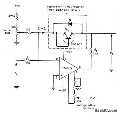
Suitable for positive input voltages. Negative feedback is applied to opamp through diode-connected transistor, with additional diode D protecting transistor from excessive inverse voltage caused by wrong input polarity. For negative inputs, reverse transistor and diode connections. Article gives design equations and application procedures.-G. B. Clayton, Experiments with Operational Amplifiers, Wireless World, Jan. 1973, p 33-35. (View)
View full Circuit Diagram | Comments | Reading(797)
SEISMIC_RADIO_BEACON(THRESHOLD_CIRCUIT)
Published:2009/7/13 22:27:00 Author:May

This threshold circuit is fed by a geophone amplifier and is actuated by seismic activity, as picked up by a geophone. The threshold is adjustable. (View)
View full Circuit Diagram | Comments | Reading(1758)
SYLLABIT_VOX
Published:2009/7/13 22:26:00 Author:May

Provides instantaneous radiotelephone speech communication without conventional V0X relays. Switching transistors eliminate contact-bounce problems of relays. Designed for use with Drake T-4XB and R-4B transmitter and receiver. Also gives true breakin CW keying. Since only words and syllables of words go on air, there are no VOX RF transients and no extraneous local noise. Operating bias for final amplifier is applied only during transmission; at other times, final amplifier tubes are completely cut off. Diodes CR4-CR7, CR9, and CR11 are 1N4004 or equivalent. All other diodes are 1N914 or equivalent. RF choke is 2.5 mH rated 100 mA. Article describes operation in detail and gives installation and setup procedures.-R. W. Hitchcock, Syllabic V0X System for Drake Equipment, Ham Radio, Aug. 1976, p 24-29. (View)
View full Circuit Diagram | Comments | Reading(1020)
SEISMIC_RADIO_BEACONAUDIO_VCO_AND_BUFFER
Published:2009/7/13 22:25:00 Author:May
This audio and VCO buffer is fed by a geophone amplifier and produces a tone modulated by seismic activity, as picked up by a geophone. (View)
View full Circuit Diagram | Comments | Reading(1386)
900_W_FULL_WAVE
Published:2009/7/13 22:24:00 Author:May

Combination of bridge rectifier, pulse transformer, and triac allows look pot RT to control power to resistive load on both positive and negative half-cycles,Triac is triggered through transformer by 2N4870 UJT,-D.A. Zinder,″Unijunction Trigger Circuits for Gated Thyristors,”Motorola, Phoenix, AZ,1974,AN-413,p 3. (View)
View full Circuit Diagram | Comments | Reading(3702)
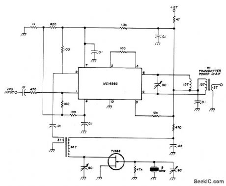
5_555_MHz_VFO
Published:2009/7/13 22:24:00 Author:May

Controls both receiver and transmitter of low-power transceiver for 20 meter amateur band. L1 is 3.5 μH wound on 6mm ceramic form without tuning slug. Number of turns is adjusted to obtain exact inductance. JFET can also be 2N4416 or Motorola MPFl02. VFO is buffered with single-stage feedback amplifier using pair of 2N3904 transistors (transistor type is not critical). Article also gives other circuits of transceiver.-W. Hayward, Low-Power Single-Band CW Transceiver, Ham Radio, Nov. 1974, p 8-17.
(View)
View full Circuit Diagram | Comments | Reading(2585)
300_mA_STEP_DOWN_BATTERY_FOUR_CELL_NiCd_CHARGER
Published:2009/7/13 22:23:00 Author:May

Low-current battery-charger circuits are required in hand-held products such as palmtop, pen-based, and fingertip computers. The charging circuitry for these applications must use surface-mount components and consume minimal board space. The LTC1174 circuit shown provides both of these features. The LTC1174 is a current-mode, step-down switching regulator with a low-loss internal P-channel MOSFET power switch. In this circuit, the peak switch current is programmed to 600 mA. The average charging current is determined by the choice of inductor value and the actual battery voltage, according to the equation. The voltage feedback resistor network is set for an output voltage of 7 Y. NiCd cells have a nominal voltage of 1.2 V, a discharged voltage of 0.9 V, and a fully charged voltage of 1.5 V. A four-cell NiCd pack's voltage will range from 3.6 to 6 V, depending upon its state of charge. When it is attached to the charger, it will pull the output voltage below 7 V and place the LTC1174 into current-limited operation at about 300 mA with the 50-μH inductor shown. Diode D2 prevents the batteries from discharging through the divider network when the charger is shut down by bringing the SHUTDOWN pin low. Less than 10 μA of current is drawn from the sup-ply when the charger is shut down.
(View)
View full Circuit Diagram | Comments | Reading(703)
SEISMIC_RADIO_BEACON_GEOPHONE_AMPLIFIER
Published:2009/7/13 22:23:00 Author:May


This geophone amplifier and buffer was used as part of an amateur radio beacon that monitors seismic activity in an earthquake-prone area of the United States.
(View)
View full Circuit Diagram | Comments | Reading(2926)
DOUBLE_BALANCED_MIXER
Published:2009/7/13 22:23:00 Author:May
Used in 80-meter SSB transceiver on both transmit and receive. Local oscillator input of 5-5.5 MHz is pro-vided by VFO. SSB signal for receive comes from two-stage MOSFET RF amplifier-D. Hembling, Solid-State 80-Meter SSB Transceiver, Ham Radio, March 1973, p 6-17.
(View)
View full Circuit Diagram | Comments | Reading(0)
CUBE_GENERATOR
Published:2009/7/13 22:21:00 Author:May

Combin ation of temperature-compensated opamp log converter and antilog converter generates output signal eo proportional to cube of input signal ei. Article gives design equations.-G. B Clayton, Experiments with Operational Amplifiers, Wireless World, Feb. 1973, p 91-93.
(View)
View full Circuit Diagram | Comments | Reading(1547)
LINEAR_SAWTOOTH_WAVEFORM_GENERATOR_CIRCUIT
Published:2009/7/13 22:20:00 Author:May
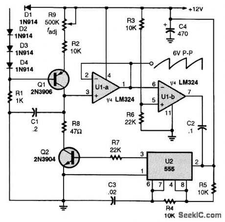
In this circuit, Q1 is a constant-current source, whose output is controlled by R9. C1 charges linearly, and follower U1-a drives comparator U1-b. When the threshold set by R3 and R6 is reached, U1-b changes state and triggers pulse generator U2, gating on Q2 and discharging C1 through R8.The cycle then repeats. The period is approximately 8 x C1/I1, where I1, is the collector current of Q1, as set by R9 and the base bias on Q1. (View)
View full Circuit Diagram | Comments | Reading(1514)
80_dBV_INPUT_RANGE
Published:2009/7/13 22:18:00 Author:May

Logamp using Texas Instruments SN56502 or SN76502 in combination with three SN52741 opamps can handle input voltage range greater than 80 dB with respect to 1 V P-P. Inputs are limited by reducing supply voltages of input amplifiers to 14 V.Gains of input amplifiers are adjusted to achieve smooth transitions.- The Linear and Interface Circuits Data Bookfor Design Engineers, Texas Instruments, Dallas, TX, 1973, p 7-45. (View)
View full Circuit Diagram | Comments | Reading(794)
LINEAR_SAWTOOTH_GENERATOR
Published:2009/7/13 22:17:00 Author:May


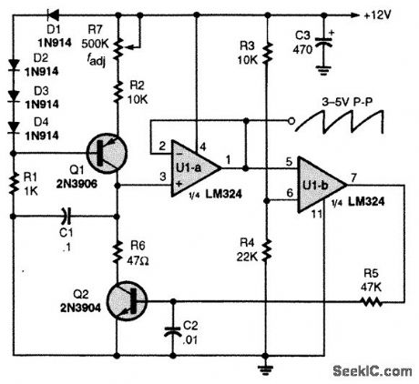
Q1is connected in a simple constant-current generator circuit. The value of Q1's emitter resistor sets the constant-current level flowing from the transistor's collector to the charging capacitor (C1).One op amp of an LM324 quad op amp IC, U1-a, is connected in a voltage-follower circuit. The input impedance of the voltage follower is very high and offers little or no load on the charging circuit. Thefollower's output is connected to the input of U1-b, which is configured as a voltage comparator. The comparator's other input is tied to a voltage divider, setting the input level to about 8 V. The output of U1-b at pin 7 switches high when the voltage at its positive input, pin 5, goes above 8 V. That turns on Q2, discharging C1. The sawtooth cycle is repeated over and over as long as power is applied to the circuit. The sawtooth's frequency is determined by the value of C1 and the charging current supplied to that capacitor. As the charging current increases, the frequency also increases, and vice versa. To increase the generator's frequency range, decrease the value of C1, and to lower the frequency, increase the value of Cr. The output is about 3 to 5 V. (View)
View full Circuit Diagram | Comments | Reading(0)
600_W_TRIGGERED_SCR
Published:2009/7/13 22:15:00 Author:May

2N4154 SCR is operated from DC output of bridge rectifier and triggered by MPT32 at setting determined by position of 300K pot. Circuit provides full-wave DC control of lamp and other loads up to 600 W, using relaxation oscillator operating from DC source.- SCR Power Control Fundamentals, Motorola, Phoenix, AZ, 1971, AN-240, p 6. (View)
View full Circuit Diagram | Comments | Reading(1061)
PRECISION_Li-ION_BATTERY_CHARGER
Published:2009/7/13 22:14:00 Author:May

An alternative to using expensive 0.25-percent precision resistors is presented in this battery-charger design, which adds two 1-percent resistors and two jumpers to the charger.In constant-voltage-mo de charging, a lithium-ion cell requires 4.1 V ±50 mV. The 1.2-percent requirement represents a tight tolerance. In a regulation loop where a voltage divider is compared against a reference, the accuracy is typically achieved by selecting a 0.7-percent reference and a volt-age divider with 0.25-percent tolerance resistors. Unfortunately, 0.25-percent precision resistors cost three times as much as 1-percent resistors and have very long lead times. One solution for moderate-volume production involves adding two 1-percent resistors and two jumpers to the charger circuit (see the figure). The jumpers are removed as necessary to bring the constant voltage to the required accuracy of 1.2 percent. The charger selected for this example is the LT1510. There are three lithium-ion cells in the. battery. After a value is selected for R4 the values for R1, R2, and R3 can be calculated using the equations given. K is the relative change required for a circuit with all of its tolerances in one direction. For example, in the case of a 0.5-percent reference and two 1-percent resistors, the total tolerance is 2.5 percent. To bring it back to 1.2 percent, the percentage change required is 2.5 percent - 1.2 percent 1.3 percent, and K =0.013. The jumpers (J1 and J2) must be opened based on the following:If VOUT is K/2 below nominal, remove J1.If VOUT is K/2 above nominal, remove J2.The following values were calculated: R1 = 4.99 kΩ, R2 = 324Ω,R 3=80.6 ,Ω and R4= 20 KΩ The voltage below which jumper J1 should be opened is 12.34 V -1.3 percent /2 = 12.22 V. The voltage above which jumper J2 should be opened is 12.34 V + 1.3 percent /2 = 12.42 V. (View)
View full Circuit Diagram | Comments | Reading(1813)
| Pages:675/2234 At 20661662663664665666667668669670671672673674675676677678679680Under 20 |
Circuit Categories
power supply circuit
Amplifier Circuit
Basic Circuit
LED and Light Circuit
Sensor Circuit
Signal Processing
Electrical Equipment Circuit
Control Circuit
Remote Control Circuit
A/D-D/A Converter Circuit
Audio Circuit
Measuring and Test Circuit
Communication Circuit
Computer-Related Circuit
555 Circuit
Automotive Circuit
Repairing Circuit