
Circuit Diagram
Index 673
HALF_WAVE_AC_CONTROL
Published:2009/7/13 23:08:00 Author:May

Motorola 4N26 optoisolator serves as interface for static series switch in gate circuit of 2N5064 SCR. When logic input goes high, optoisolator is energized and first SCR is triggered on. Resulting current turns on power SCR for passing load current on that positive half-cycle of AC line voltage. When logic goes low, load current stops at next zero crossing of AC source. 5mA of isolated DC control current thus controls up to 16 A for half-wave load.-A. Pshaenich, Interface Techniques Between Industrial Logic and Power Devices, Motorola, Phoenix, AZ, 1975, AN-712A, p 16. (View)
View full Circuit Diagram | Comments | Reading(1869)
CABLE_REFLECTION_TESTER
Published:2009/7/15 23:40:00 Author:Jessie
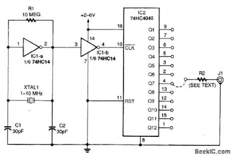
This device is a square-wave generator and frequency divider. A square-wave generator supplies a signal to the cable through a resistance (R2) equal to the characteristic impedance of the cable. Any reflections caused by mistermination will show up on a scope hooked to J1. IC2 acts as a frequency divider to produce various pulse rates for testing long and short cable. (View)
View full Circuit Diagram | Comments | Reading(1595)
4_KC_SCALER
Published:2009/7/13 23:08:00 Author:May

Drives glow tube at maximum possible rate. Uses single-shot mvbr and step-up transformer Q1 to obtain 300-V pulses required to drive glow tube. Single drive pulse is fed simultaneously to both guides of tube.-H. A, Kampf, Increasing Counting System Reliability Electronics.32:37,p112-1l3. (View)
View full Circuit Diagram | Comments | Reading(432)
RANDOM_TIME_PULSES
Published:2009/7/15 23:39:00 Author:Jessie

When gate is opened by noise, sine wave steps electron beam of Burroughs tube through its ten sections. Transistor connected to each target produces voltage pulse whose magnitude depends on potentiometer setting, giving sequence of different voltages in output. When beam reaches position 9, pulse is fed back to dose the gate.-C. V. Jakowatz and Q. M. White, Self-Adoptive Filter Finds Unknown Signal in Noise, Electronics, 34:7, p 117-119. (View)
View full Circuit Diagram | Comments | Reading(781)
BATTERY_TRICKLE_CHARGER
Published:2009/7/13 23:08:00 Author:May

The circuit is built around an LM317T adjustable voltage regulator. Its output voltage (VOUT) is determined by the formula VOUT= l.25 (1+R2/R1). I chose a 10-kΩ resistor for R1 and a 100-kΩ resistor for R2 to allow for a little wasted current flow (around 125 μA). This will develop 13.75 V between the output terminal and ground. R3 and a diode prevent burnout if the terminals are shorted or reversed, and prevent battery discharge in the event that the regulator is disconnected from the main power supply. The capacitor is optional but will make life easier on the chip under an extreme charging cycle. With proper heat sinking, the IC is capable of carrying 1.5 A to the battery. The circuit can be left hooked to the battery all of the time and will not overcharge it. (View)
View full Circuit Diagram | Comments | Reading(2324)
FREE_RUNNING_CASCODE_MULTIVIBRATOR
Published:2009/7/15 23:38:00 Author:Jessie

Output signal at cathode of V1 is nearly perfect square wave, either positive or negative depending on setting of potentiometer. -C. Sing, Advantages of Free-Running Cascode Multivibrators, Electronics, 37:5, p 28-29. (View)
View full Circuit Diagram | Comments | Reading(491)
MULTICONDUCTOR_SHORT_OPEN_CABLE_TESTER
Published:2009/7/15 23:38:00 Author:Jessie
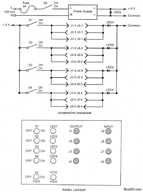
Frequent or regular testing of multiconductor cables terminated in multipin conductors can be a tedious, if not impossible, task. This is especially true if the cables must be tested for both open and short circuits for all of the various combinations of conductors. The inexpensive circuit shown in the figure simplifies the task. In operation, a pair of connectors is selected to match the pair of connec-tors installed on each of the cables to be tested. A single-pole/single-throw (SPST) toggle switch is provided for each conductor of whichever cable in the system has the greatest number of conductors. One conductor of each of the output connectors is connected in parallel to the anode of an LED.One LED is required for each conductor of the cable that has the greatest number of conductors. The cathodes of the LEDs are tied together and connected to the common side of the 5-V power supply.At the beginning of a test, all of the switches are turned off. First, one turns on power switch S5 and verifies that LED5 illuminates. Then one turns on switches S1 through S4, one at a time. Only the LED corresponding to the switch that is on should illuminate. An open conductor in the test cable is indicated if the corresponding LED is not illuminated. A short circuit is indicated if any other than the corresponding LED is illuminated. (View)
View full Circuit Diagram | Comments | Reading(961)
LOGIC_CONTROLS_15_A_LOAD
Published:2009/7/13 23:06:00 Author:May

Load is energized when logic input drops to 0. Can be used to drive solenoid or electromagnet from 48-VDC supply, for stopping paper tape in high-speed tape reader. If relay is to be activated by high or 1 level, add inverter at input as shown.-D. D. Mickle, Practical Computer Projects, 73 Magazine, Jan. 1978, p 92-93.
(View)
View full Circuit Diagram | Comments | Reading(646)
HIGH_SPEED_VOX
Published:2009/7/13 23:05:00 Author:May

Use of switching transistors for rapid, silent voice-controlled switching of transmitter-receiver functions improves on-the-air effectiveness of SSB station. Conversation is essentially the same as when using telephone. Each set of contacts that would open or close single circuit in relay-type VOX is replaced by switching transistor. TR switch is diode-biased antenna gate in which actual switching takes place 200 μs before RF appears, being accomplished by forward-biasing diode with DC voltage. Input to LM3900 is through high-pass filter. Operation of similar solid-state VOX circuit is described in detail in earlier article by same author (see author index),-H. R. Hildreth, Syllabic VOX System for the Collins S-Line, Ham Radio, Oct. 1977, p 29-33. (View)
View full Circuit Diagram | Comments | Reading(634)
THERMAL_MONO
Published:2009/7/15 23:37:00 Author:Jessie

Accurate pulse periods of 15 sec to 2 minutes are produced by thermal mono using silicon resistor (Sensistor) whose resistance varies with temperature, power, and time. Used as timer to turn on plate supply 30 sec after filament supply.-L. L. Kleinberg, Sensistor Produces Long, Reliable Pulses, Electronics, 37:31, p 51-52. (View)
View full Circuit Diagram | Comments | Reading(579)
SUPERREGENERATIVE
Published:2009/7/15 23:37:00 Author:Jessie
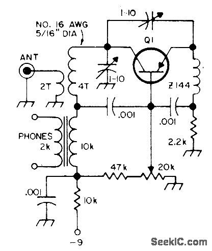
Simple single-transistor superregenerative receiver is adequate for copying many local signals in 2-meter amateur band. With components shown, tuning range is about 90 to 150 MHz. Transistor can be GE-9 or HEP-2.-Circuits, 73 Magazine, Feb. 1974, p 100. (View)
View full Circuit Diagram | Comments | Reading(1945)
SCANNER_WITH_SEARCHBACK
Published:2009/7/13 23:03:00 Author:May

Combines scanning between two repeater channels with periodic searchback, to prevent scanner from locking on one of channels during long periods of use NE555 timer is added to squelch recognition circuit to provide automatic control of scanner so both frequencies are checked at least every 15 s,If scanner is extended to monitor four channels, none are unguarded for more than 1 min,Article shows how receiver section of transceiver is modified for diode switching by scanner of oscillator crystals for individual channels.-P, Shreve, Two-Channel Scanner for Repeater Monitoring, Ham Radio, Oct,1976, p48-51. (View)
View full Circuit Diagram | Comments | Reading(596)
NONCUTOFF_MONOSTABLE
Published:2009/7/15 23:35:00 Author:Jessie

Optimum operating conditions are achieved by keeping amplifiers connected to current sources continuously. With constant input voltage, triggering makes threshold level shift. Diodes in feedback loop improve switching speed. -H. Inose, Y. Yoshida, and H. Tada, Noncutoff Circuits Improve Trigger Switching, Electronics, 35:30, p. 36-39. (View)
View full Circuit Diagram | Comments | Reading(619)
STEERING_FOR_REVERSIBLE_DECADE_COUNTER
Published:2009/7/13 23:03:00 Author:May


Consists of four R-C coupled complementary saturated flip-flops Q1-Q8. Symmetrical npn steering fransistors Q9 through Q16, coupled between collectors of flip-flops, are used as trigger current amplifiers and for steering when counting up or down.-R..D. Carlson, Steering Circuits Control Reversible Counters, Electronics, 33:1, p 86-88. (View)
View full Circuit Diagram | Comments | Reading(641)
CABLE_SHORT_DETECTOR
Published:2009/7/15 23:34:00 Author:Jessie
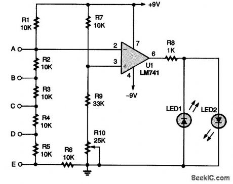
A five-input short-detector circuit can be used to check long runs of a two- to five-wire cable for shorts between any of the wires. An LM741 op-amp IC, U1, is connected in a comparator circuit. The inverting input (pin 2) of U1 is connected to a +9-V source and a series of six resistors, while the noninverting input (pin 3) of the op amp is connected to an adjustable voltage-divider circuit. To use the circuit, potentiometer R10 should be used to set the voltage at pin 3 to a slightly more negative voltage than that at pin 2; U1's output will swing low, lighting LED1. Make that adjustment slowly until LED1 just barely turns on. Then connect one end of a cable to points A to E. When any of resistors R2 to R6 are shorted out, the voltage at pin 2 will go negative with respect to pin 3. That will make the op amp's output go positive, which will light LED2, indicating a short in the cable. (View)
View full Circuit Diagram | Comments | Reading(2339)
VFO_WITH_DIRECT_CONVERSION_DETECTOR
Published:2009/7/15 23:34:00 Author:Jessie

Used in demodulating SSB and CW signals. Incoming signal is heterodyned with VFO output to give direct conversion to audio. Audio filter R4-C7-C8 allows only AF components to be transferred to audio amplifier Q2. Oscillator can be operated alone for other purposes by removing jumper between output terminals 2 and 3, then applying +24 V to terminal 3 and negative supply to terminal 4. Load on low-level output of oscillator has negligible effect on frequency, Load on high output may change frequency, but this can be corrected by retuning oscillator if load is constant. Values shown are for 80-meter band.-E. M. Noll, FET Principles, Experiments, and Projects, Howard W. Sams, Indianapolis, IN, 2nd Ed., 1975, p 165-173.
(View)
View full Circuit Diagram | Comments | Reading(822)
10_METER_PBEAMP
Published:2009/7/15 23:32:00 Author:Jessie
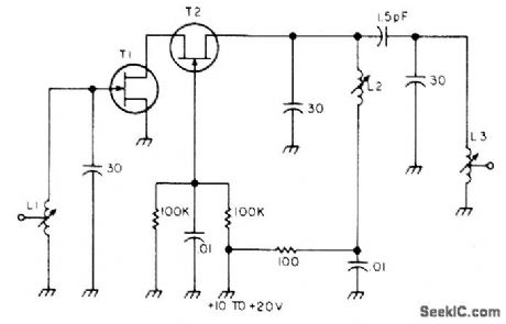
Simple preamp can also be used on 2 meters with appropriate change of coils. Needs no neutralization. Developed for use with receiver capable of receiving satellite transmissions on 29.45 to 29.55 MHz. Transistors can be MPF 102, MPF 106, or 2N4416. All coils are 1.2 μH having 7 turns No. 26 enamel on 3/16-inch slug-tuned form. L1 and L3 have tap at 3 turns. -G. L. Tater, CQ OSCAR 7, 73 Magazine, Feb. 1975, p 54-56 and 58-60. (View)
View full Circuit Diagram | Comments | Reading(670)
CABLE_TESTER_RECEIVER
Published:2009/7/15 23:31:00 Author:Jessie
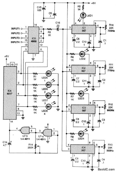
The four inputs are connected to four input contacts of a quad bilateral switch, IC5, with the out-put contacts tied together and connected to the inputs of the 567 decoders through R9 and C16. The bilateral switch's four control inputs are operated by IC6, a 4017 decade counter IC, which is driven by a low-frequency oscillator made up of two gates of IC7, a quad two-input NAND gate. Four LEDs, LED 5 through LED8, are connected to IC6's four outputs and indicate which input is being checked, just as in manual mode. When LED5 is on, input 1 is switched through to the four decoder circuits. The decoder that responds, by lighting its LED, indicates which output-700, 775, 880, or 950 Hz-is connected to that input. Resistor R14 sets the input-stepping rate, which should be slow enough for recording. (View)
View full Circuit Diagram | Comments | Reading(1123)
MORE_EFFICIENT_BATTERY_CHARGER
Published:2009/7/13 22:57:00 Author:May

The project at hand was to build a small, efficient, inexpensive, full-function battery charger that could charge 2 to 10 NiCd or NiMH cells. A switching regulator that could be set up as a constant-current source was needed. Connecting the negative end of the battery directly to ground provides more voltage and reduces IR losses. Linear Technology's LTC1148HV synchronous step-down switching regulator fills this role because it is more than 90 percent efficient, and it features two current sense inputs (Sense+ and Sense-) and a current control pin (Ith) that has a dc input linearly related to the maximum coil current (Fig. 1). For example, with a low, commonly available 0.1-Ω sense resistor and Ith connected to the 2-JV reference output of the MAX713, the peak coil current is set to 1.55 A. The average current will still vary with output voltage, but this can be compensated for by feeding back some of the output voltage to Ith The constant-voltage regulation loop of the LTC1148 is disabled once the voltage divider (R2 and R7) forVFB is set above the highest voltage that the battery is going to reach during charge. With the battery above the constant voltage regulation point, the switching regulator will supply no current. If a trickle charge current is desired, a switch (USA) and a resistor (R14) can be added that supply the desired current directly from the primary dc source (Vin)-a simple wall cube-when the MAX713 controller terminates fast charge or during battery undervoltage condition at startup. (View)
View full Circuit Diagram | Comments | Reading(1362)
DUAL_GATE_MOSFET_MIXER
Published:2009/7/15 23:30:00 Author:Jessie
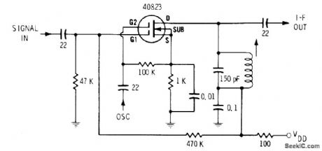
RF and oscillator signals are applied to gates G1 and G2 for mixing in MOSFET. Choice of sum or difference frequency is determined by values used in tank circuit and by tuned circuits of IF amplifier.-E.M. Noll,″ FET Principles, Experiments, and Projects,″ Howard W. Sams, Indianapolis, IN, 2nd Ed., 1975,p 141-142. (View)
View full Circuit Diagram | Comments | Reading(1900)
| Pages:673/2234 At 20661662663664665666667668669670671672673674675676677678679680Under 20 |
Circuit Categories
power supply circuit
Amplifier Circuit
Basic Circuit
LED and Light Circuit
Sensor Circuit
Signal Processing
Electrical Equipment Circuit
Control Circuit
Remote Control Circuit
A/D-D/A Converter Circuit
Audio Circuit
Measuring and Test Circuit
Communication Circuit
Computer-Related Circuit
555 Circuit
Automotive Circuit
Repairing Circuit