
Circuit Diagram
Index 665
SINGLE_BALANCED__MIXER
Published:2009/7/15 23:26:00 Author:Jessie

Uses RCA CA3028A differential amplifier U1 to provide conversion gain of about 30 dB for signal inputs up to 120 MHz Values of tuned circuits depend on frequency used, Unmarked resistors are on IC.-D. DeMaw, Understanding Linear ICs, QST, Feb. 1977, p 19-23. (View)
View full Circuit Diagram | Comments | Reading(1076)
DIAMOND_BRIDGE_ANALOG_SWITCH
Published:2009/7/14 0:55:00 Author:May

Analog signals up to 3 V P-P are switched in less than 3 ns to meet requirements of multiplexer and sample-and-hold portions of 100 Mb/s PCM telemetry encoder. Symmetrical drive circuits turn four-transistor diamond bridge on and off at 20-MHz clock frequency. Transient-coupled pullback transistors Q5 and Q9 speed turnoff. Typical rise time is 1,5 ns and fall time is 2 ns for 1-VDC analog input.-W. A. Vincent, Diamond Bridge Improves Analog Switching, EDN Magazine, Feb 15, 1971, p 41-42. (View)
View full Circuit Diagram | Comments | Reading(1431)
MIXER_LOAD_DIFFERENTIAL_AMPLIFIER
Published:2009/7/15 23:25:00 Author:Jessie
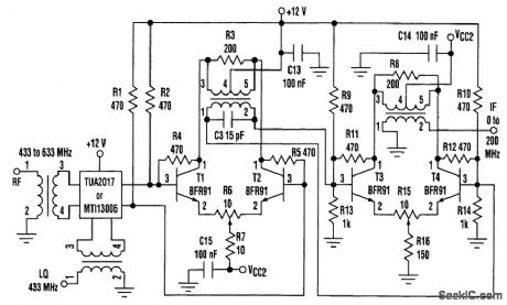
Two different amplifier stages are used as the load of the mixer TUA2017 or MTl13006 (products developed by Siemens Co.). The LQ frequency is fixed at 483 MHz, because a commercial SAW oscillator at 483 MHz can be used as a local oscillator. If the RF frequency is swept from 433 to 633 MHz, then the IF frequency also is swept from 0 to 200 MHz. Compared to a passively loaded mixer, this combination of mixer and differential amplifiers exhibits excellent performance. The relative amplitude (amplitude difference between the fundamental frequency and the largest distortion frequency) is typically at least 50 dB. But it is only 30 dB (or less) in the case of a passive load mixer. Resistors R4, R5, R11, and R12 are used as the shunt feedback to obtain the flat output amplitude when the RE frequency is swept. The amplitude ripple with the IF bandwidth (0 to 200 MHz) is less than 0.5 dB. (View)
View full Circuit Diagram | Comments | Reading(865)
ANALOG_SWITCH_PROTECTION_
Published:2009/7/14 0:54:00 Author:May

Current-limiting resistors are used in series with sections of DG300 dual analog switch to limit contact currents to 30 mA continuous or 100 mA pulsed for less than 1 ms. Values of limiting resistors depend on supply voltage used and are therefore determined by experimentation. Technique is suitable for applications in which DG300 serves for charging and discharging capacitor.- Analog Switches and Their Applications, Siliconix, Santa Clara, CA, 1976, p 7-81. (View)
View full Circuit Diagram | Comments | Reading(669)
SWITCHING_OPAMP
Published:2009/7/14 0:53:00 Author:May
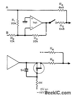
Circuit provides change-over function when only single pair of contacts is available. With switch open, input A goes to output. With switch closed, input B goes to out-put and signal of input A is inverted by opamp so as to cancel direct signal A. Gain is unity for both output signals. Switch can be replaced by FET as in lower diagram; here, capacitor pre vents FET from cutting off during positive half-cycle above about 100 Hz. In multichangeover applications, opamp could be section of programmable opamp.-M. J. Sells, Electronic Changeover Switching, Wireless World, Dec.1974, p 503. (View)
View full Circuit Diagram | Comments | Reading(756)
FET_ANALOG_SWITCH
Published:2009/7/14 0:51:00 Author:May

Simple level-shifting driver provides analog switching. Input of logic 1 makes emitter and collector current flow in input PNP transistor, for shifting from logic to -15 V. This current makes NPN transistor turn on so its collector is -15 V, diode is forward-biased, and FET gate is about -14.3 V. At logic 0, both transistors are off and driver output is at +15 V. Diode is now reverse-biased, turning FET on to provide desired switching action between outputs 1 and 2.-J. Cohen, Solid-State Signal Switching: Ifs Getting Better All the Time, EDN Magazine, Nov. 15, 1972, p 22-28. (View)
View full Circuit Diagram | Comments | Reading(1967)
LATCHING_SPDT
Published:2009/7/14 0:50:00 Author:May

DG200 CMOS analog switch is driven through pair of NAND gates connected for logic inputs. With inputs normally low, both switches are held in predetermined states. When either input receives high command pulse, switches assume states given in truth table. Both switches are off when both inputs are held high; after release of high commands, last input to go low determines states of switches.- Analog Switches and Their Applications, Siliconix, Santa Clara, CA, 1976, p 7-69. (View)
View full Circuit Diagram | Comments | Reading(699)
FERRITE_CORE_SWITCHING
Published:2009/7/14 0:50:00 Author:May

Darlington transistor driven by low-power current stage serves for saturating groups of ferrite cores in phased arrays for radar systems or in read/write core switching for memory systems. Circuit provides fast rise and fall times.- Designer's Guide to Power Darlingtons as Switching Devices, Unitrode, Watertown, MA, 1975, U-70, p 4. (View)
View full Circuit Diagram | Comments | Reading(821)
VIDEO_SWITCH
Published:2009/7/14 0:49:00 Author:May

2N4391 FETs provide ON resistance of only 30 ohms and OFF impedance less than 0.2 pF, to give performance comparable to that of ideal high-frequency switch. Attenuation is greater than 80 dB at 100 MHz. Insertion loss is about 6 dB.- FET Databook, National Semiconductor, Santa Clara, CA, 1977, p 6-26-6-36. (View)
View full Circuit Diagram | Comments | Reading(0)
FOUR_CHANNEL_COMMUTATOR
Published:2009/7/14 0:48:00 Author:May
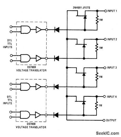
2N401 JFETs give ON resistance of less than 30 ohms for each channel along with low OFF current leakage, DS7800 voltage translators provide gate drives of 10 V to -20 V for JFETs while giving DTL/TTL compatibility, - FET Databook, National Semiconductor, Santa Clara, CA, 1977, p 6-26-6-36. (View)
View full Circuit Diagram | Comments | Reading(874)
DPDT_FET
Published:2009/7/14 0:47:00 Author:May

With ON resistance of several ohms and OFF resistance of thousands of megohms, drain-source channel of field-effect transistor makes ideal low-frequency switch. Transistor capacitances are detrimental to high-frequency signal isolation and limit response times.- Low Frequency Applications of Field-Effect Transistors, Motorola, Phoenix, AZ, 1976, AN-511A, p 5. (View)
View full Circuit Diagram | Comments | Reading(940)
ANALOG_WITH_HIGH_TOGGLE_RATE
Published:2009/7/14 0:46:00 Author:May

Simple commutator circuit provides low-impedance gate drive to PN4091 FET analog switch for both ON and OFF drive conditions. For high-frequency signal handling, circuit also approaches ideal gate drive conditions by providing low AC impedance for OFF drive and high AC impedance for ON drive.- FET Databook, National Semiconductor, Santa Clara, CA, 1977, p 6-26- 6-36. (View)
View full Circuit Diagram | Comments | Reading(700)
INPUT_ATTENUATOR
Published:2009/7/16 1:50:00 Author:Jessie

Low-distortion automatic input attenuator for modern communication receiver is activated at input signal levels above 100 μV. For range of 1-30 MHz, use PIN diodes such as HP5082-3081, Intermodulation distortion products of attenuator are about 85 dB down for two 1-V signals.-U. L. Rohde, 0ptimum Design for High-Frequency Communications Receivers, Ham Radio, Oct. 1976, p 10-25.
(View)
View full Circuit Diagram | Comments | Reading(1157)
DIFFERENTIAL_ANALOG_SWITCH
Published:2009/7/14 0:45:00 Author:May

NPD5566 dual JFETs provide high accuracy for differential multiplexer because JFET sections track at better than ±1% over wide temperature range, close tracking reduces errors due to common-mode signals Values of resistors depend on application and on type of opamp used.- FET Databook, National Semiconductor, Santa Clara, CA, 1977, p 6-26-6-36. (View)
View full Circuit Diagram | Comments | Reading(0)
AND_LOGIC_GATE
Published:2009/7/16 1:50:00 Author:Jessie

And/or gate using pnp input transistors and npn output transistors is followed by three-transistor inverting output stage. Gate has fan-in of 5.-C. R. Cook, Jr., and B. M. Martin, New semiconductor Networks Reduce System Complexity, Electronics, 37:2, p 25-29. (View)
View full Circuit Diagram | Comments | Reading(506)
BRIDGE_GATE_TEST_CIRCUIT
Published:2009/7/16 1:49:00 Author:Jessie

Two-state a-c bridge having biased tunnel-diode in one arm can be used as gale when balanced in one of its stable states.-F. W. Kantor, Tunnel-Diode Gale has Subnanosecond Rise Time, Electronics, 35:15, p 62-64. (View)
View full Circuit Diagram | Comments | Reading(531)
TEACHING_MACHINE_REWARD_GATE
Published:2009/7/16 1:48:00 Author:Jessie

Astable and monostable multivibrators feed and gale that triggers reward-dispensing device(such as candy dispenser) when number of correct answers exceeds preset percentage of random Probability.Circuit may also give 100% reinforcement for correct response but with candy reward only at spaced intervals.-G. S. Pennington, Jr. and J. A. Boehm, III, Gate Varies Rewards from Teaching Machine, Electronics, 39;10, p 92-93. (View)
View full Circuit Diagram | Comments | Reading(563)
MULTIEMITTER_TRANSISTOR_AND_OR_LOGIC
Published:2009/7/16 1:48:00 Author:Jessie

Circuits may be coupled either directly or by multi-emitter transistor and gates. Components show promise for integrated circuits.-P. M. Thompson, Logic Principles for Multi-emitter Transistors, Electronics, 3637, p 25-29. (View)
View full Circuit Diagram | Comments | Reading(767)
TRANSFORMER_DRIVE_FOR_SWITCHING_TRAN_SISTOR
Published:2009/7/14 0:44:00 Author:May
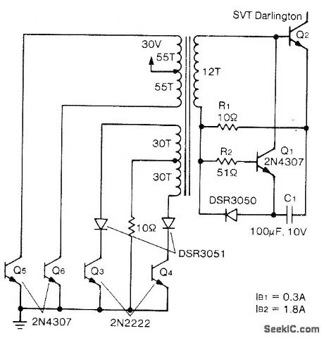
Transformer provides isolated base drive for high-speed high-power TRW SVT6062 power Darlington Q2. When 12-V secondary switches positive, C1 charges rapidly, after which base drive current is maintained at level determined by base-emitter voltage of Q2 and value of R1. During turnoff, transformer secondary goes to zero due to shorting of transformer primary by O3 and Q4. Base of Q1 is then forward-biased by capacitor and turned on, discharging C1 through base-emitter path of Q2-D. Roark, Base Drive Considerations in High Power Switching Transistors, TRW Power Semiconductors, Lawndale, CA, 1975, Application Note No. 120, p 6. (View)
View full Circuit Diagram | Comments | Reading(869)
FAST_ON_AND_OFF
Published:2009/7/14 0:42:00 Author:May

Driver Q1 is low-power device with fast switching time, while power transistor Q2 handles power dissipation and amperes of current being switched. Used in TTL circuits requiring fast solid-state switches having known and repeatable switching times. Cur-rent reaches maximum in about 50 ns.-C. Venditti, Fast Power Switch Self-Corrects for Degradation, EDN Magazine, Jan. 20, 1975, p 59-60. (View)
View full Circuit Diagram | Comments | Reading(610)
| Pages:665/2234 At 20661662663664665666667668669670671672673674675676677678679680Under 20 |
Circuit Categories
power supply circuit
Amplifier Circuit
Basic Circuit
LED and Light Circuit
Sensor Circuit
Signal Processing
Electrical Equipment Circuit
Control Circuit
Remote Control Circuit
A/D-D/A Converter Circuit
Audio Circuit
Measuring and Test Circuit
Communication Circuit
Computer-Related Circuit
555 Circuit
Automotive Circuit
Repairing Circuit