
Circuit Diagram
Index 670
PRECISE_LOW_CURRENT_SOURCE
Published:2009/7/16 1:35:00 Author:Jessie

A current source that attains a resolution as low as 10 pA is useful in applications where a precise, low-value current is needed. When the circuit forces current into ground, the output remains within 2% of the ideal current over the ±100-nA range. Over the -4- to +3.5-V compliance range, the error that appears is less than 5%. This accuracy results from using an OP80 op amp from Precision Monolithics in the feedback loop. The OP80 has an IB of 200 mA typical.
For a given voltage (Vin), amp U1A generates an output voltage so that the current through R5 equals Vin divided by R5 (10 MΩ). This current causes a voltage drop across R5, which is sensed by the unity-gain differential amp (U1B and U2). That amp's output is connected to the inverting input of U1A, completing the feedback loop.
The noise in the circuit is of particular concern, especially that produced by resistor R5. The circuit is limited to low-frequency and dc applications as a result of its 400-n V/kHz noise. For applications that don't require the circuit's 10-pA output, lower values of R5 can be substituted. This will increase the bandwidth.
(View)
View full Circuit Diagram | Comments | Reading(1559)
READ_WRITE_AMPLIFIER
Published:2009/7/16 1:33:00 Author:Jessie

Each of 28 vertical circuits for coincident-flux memory consists of readout detector, bit register (flip-flop), write gate, and two-stage write amplifier-H. F. Priebe, Jr., Three-Hole Cores for Coincident.Flux Memory, Electronics, 33:31, p 94-97. (View)
View full Circuit Diagram | Comments | Reading(649)
HIGH_SPEED_TUNNEL_DIODE_BINARY
Published:2009/7/16 1:32:00 Author:Jessie
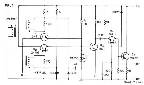
Tunnel diode with Q1-Q2, driven by series of positive or negative pulses at input repetition rates up to 140 Mc, can provide pulses capable of triggering successive pulse amplifier stages Q3, Q4, and Q5.-W. V. Harrison and R. S. Foote, Tunnel Diodes Increase Digital-Circuit Switching Speeds, Electronics, 34:32, p 154-156. (View)
View full Circuit Diagram | Comments | Reading(717)
DVM_CAPACITANCE_METER_ADAPTER
Published:2009/7/16 1:31:00 Author:Jessie
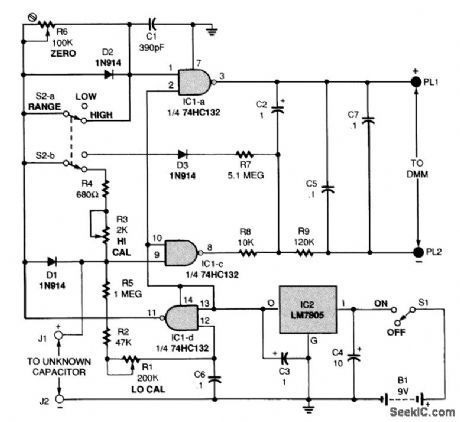
The figure shows the schematic for the capacitance meter adapter. When power switch S1 is in the ON position, an LM,7805 regulator (IC2) provides a 5-V source to the circuit. Switch 52 is used to select between the high- and low-capacitance ranges. The circuit measures from 0 to 2200 pF in its low range and from 0 to 2.2 μF in its high range. The adapter outputs 1 mV/pf in the lower range and 1 V/pF in the higher range. Those voltages would be displayed on a DMM, and would have to be read as capacitance values. Gate IC1-d is configured as a free-running oscillator whose frequency is determined by the setting of potentiometer R1. The output of IC1-d, pin 11, is a square-wave volt-age that is fed to the other two gates configured as inverters (IC1-a and IC1-c). A capacitor with an unknown value (CX) is connected across input terminals J1 and J2. Note that the positive lead of a polarized capacitor must be connected to J1. The capacitor under test charges through diode Dl on positive half cycles and discharges through R5 on negative half cycles in the low range, or through R3, R4, and R5 in the high range. In the high range, the square-wave output from IC1-d is fed directly to the inputs of the other two gates. With no capacitor connected to J1 and J2, the outputs of IC1-a and IC1-c are identical inverted versions of the input signal. The average voltage across the outputs of the gates at pins 3 and 8,In this case,is zero .With CX in place,and depending on its value,the input voltage to IC1-c,pin 9,stays higher longer than the input to IC1-a,pin 2.The output pulses from IC1-a and IC1-c are filtered and smoothed by R8,R9,C2,and C5 The average dc voltage across the outputs IS then proportional to the value of CX The circuit is a bit different in the low-range because compensation must be made for stray capacitance In the low range the output from IC1-d is fed to pin 1 of IC1-c through diode D2,which also charges C1 Capacitor C1 charges quickly and discharges slowly through potentiometer R6.The charge on C1 holds the input to IC1-a higher for a slightly longer time than would normally be the case That causes its inverted output to be low for a slightly longer time,and conversely high for a slightly shorter time Stray capacitance across input terminals J1 and J2 does the same thing to IC1-c,holding its input higher for a slightly longer time than would be the case f there were none Potentiometer R6 is adjusted so that the discharge time for C1 matches that of the stray capacitance and so cancels it out In the low range,an offset voltage is applied to the negative output terminal via D3,R7,and R8 to prevent the gates from locking together with such close trigger points (View)
View full Circuit Diagram | Comments | Reading(3122)
COUNTING_UP_TO_50_KC
Published:2009/7/13 23:20:00 Author:May


Input stage is Schmitt trigger Q1-Q2. Diode at input of interstage transistor amplifier Q3 dips base of cathode pulse.-K. Apel and P. Berweger, Miniature Gas-Filled Tubes For High-Speed Counting, Electronics, 33:8, p 46-47. (View)
View full Circuit Diagram | Comments | Reading(577)
SIREN_GENERATOR
Published:2009/7/13 23:18:00 Author:May
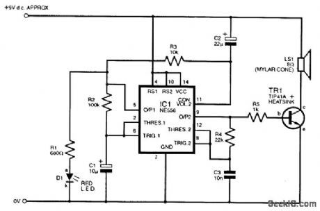
An adaptable siren generator circuit with a multitude of uses is shown. It is based around a 556 twin-timer chip, IC1. An audio tone is created by one timer section and is directly coupled to the driver transistor, TR1. The other half of the timer is used to modulate the frequency of the audio tone using the CONTROL VOLTAGE pin terminal of the audio-oscillator section, pin 11. If capacitor C2 is omitted from the circuit, a twin-tone alarm generator will be created. However, with C2 in place as shown, a wailing tone is produced. Capacitor C1 governs the rate of tone change and LED D1 flashes for extra effect. A waterproof Mylar-coned 8-Ω loudspeaker was used for LS1, and the volume can be adjusted for different impedances by altering the value of resistor R5. The circuit operates from approximately a 9-V rail. (View)
View full Circuit Diagram | Comments | Reading(2641)
LOGIC_LEVEL_SHIFTER
Published:2009/7/16 1:30:00 Author:Jessie

Common-emitter circuit of Q2 shifts logic level from +6.8 v to -6.8 v, with rise and fall limes of 60 nsec.Q3 is buffer.-G. Marosi, High-Speed Level Shifter, Electronics, 39:5, p 105. (View)
View full Circuit Diagram | Comments | Reading(1710)
COINCIDENCE_DECADE_COUNTER
Published:2009/7/13 23:18:00 Author:May

Circuit generates coincidence triggers for advancing count at any instant. Two decade schemes are shown by broken lines connected to basic counter stages. With dash-dash lines, counting proceeds in binary fashion until eighth count; at ninth count, stages 1 and 4 generate positive leading coincidence trigger and apply it to stages 2 and 3 to change them from 0 to 1, so all stages are at 1 on count 9. Next count then clears all stages to O. Dash-dot lines show coincidence for advancing the counter six units for the fourth count.-P. K. Malhotra and R. Parshad, Novel Coincidence Technique for Transistor Decode Counter, Electronics, 36:7, p 71-72. (View)
View full Circuit Diagram | Comments | Reading(814)
±35_V_SUPPLY_FOR_AUDIO_AMPLIFIERS
Published:2009/7/16 1:30:00 Author:Jessie

This supply will be found useful for operating 100-W output range. T1 = 120 V: 70 V CT at 5 A. (View)
View full Circuit Diagram | Comments | Reading(776)
ISOLATED_GATE_DRIVEFOR_TRIAC
Published:2009/7/13 23:17:00 Author:May

TIL111 optoisolator provides electrical isolation between control logic and gate drive for triac at low cost, with faster switching than is possible with relays. Transistor provides direct current drive for gate of triac. - Thyristor Gating for μp Applications,″Texas Instruments,Dallas,TX,1977, CA-191,p4-5.
(View)
View full Circuit Diagram | Comments | Reading(3308)
FULL_BINARY_ADDER
Published:2009/7/16 1:29:00 Author:Jessie

Two tunnel diodes in series perform arithmetic function of full addition.-B. Rabinovici and J. Klapper, Designing Tunnel-Diode Circuits Using Composite Characteristics, Electronics, 35:7, p 46-48. (View)
View full Circuit Diagram | Comments | Reading(726)
STEP_UP_SUPPLY_BATTERY_CHARGER
Published:2009/7/13 23:16:00 Author:May

IC1 is a step-up switching regulator that boosts Vin (nominally 5 V) as necessary to supply the combination of charging current and load current. The 5-V source must include short-circuit protection. IC2 is a high-side current-sense amplifier that monitors the charging current. Commands from the processor include. CHARGE ON/OFF and FAST/TRICKLE CHARCGE. IC2 produces an output current (OUT) equal to 10-4 of the current through sense resistor R9. Q3 and Q4 are on during a fast-charge operation, so this output current flows through the parallel combination of R11 and (approximately) R4. The resulting feedback to IC1 (pin 3) maintains the fast-charge current through R9 at 500 mA. This feedback also enables the regulator to supply as much as 500 mA of load current in addition to the fixed 500 mA of charging current. Q2 limits the battery voltage to 10 V (2 V/cell). During the fast charge, an external processor and multichannel A/D converter (ADC) must monitor the battery's terminal voltage. When the ADO senses a change of slope in this voltage, the processor terminates the fast charge by asserting a high on FAST/TRICKLE CHARGE. Q3 turns off, causing a rise in the feedback (FB) that lowers the charging current to the trickle charge rate (approximately 60 mA). If IC1 shuts down or if the load current plus charging current exceeds the capability of IC1, the R9 current reverses as current flows out of the battery. IC2 indicates the reversal by allowing R13 to pull its open-collector SIGN output high, turning off Q4 and turning on Q5. Current through R12 then produces a voltage proportional to the battery's discharge current (5 A through R9 produces a full-scale response of 3 V across R12). By integrating this voltage over time (sampling at fixed intervals and multiplying by the time interval), the A/D-processor system can monitor energy removed from the battery. Based on this measurement and the terminal-voltage measurement, the processor can then reinitiate a fast charge (by asserting FAST/TRICKLE CHARGE low) before the battery reaches its end of life.
(View)
View full Circuit Diagram | Comments | Reading(1522)
UNIVERSAL_NBS_DIODE_LOGIC_CIRCUIT
Published:2009/7/16 1:29:00 Author:Jessie

Developed National Bureau of Standards to perform all required logic perations in two computers. Uses beam power tube for amplification of 1-Mc pulses, and transformer for coupling to subsequent levels.-Y. Chu, Digital Computer Design Fundamentals, McGraw-Hill, N.Y., 1962, p 173. (View)
View full Circuit Diagram | Comments | Reading(652)
BRIDGE_RECTIFIER
Published:2009/7/16 1:29:00 Author:Jessie

This bridge circuit is intended for those cases where two unequal supply voltages are required. The lower voltage is obtained with the aid of a transformer with symmetric windings and half-wave rectification of the potential across one winding.
For the higher voltage, the potential across both windings is rectified. To that end, the output of the transformer is linked to the bridge rectifier via two electrolytic capacitors that provide isolation of the two direct voltages.
A bonus with this type of circuit is that although the two supplies can be loaded unequally, the currents through the two transformer windings are the same. Thus, the transformer is loaded symmetrically so that its full capacity can be used. Moreover, no unnecessary dissipation is in the voltage regulators.
The load on the lower voltage supply depends primarily on the rating of the transformer. The load on the higher voltage supply is limited by the reactance of C1 and C2 ( 1/2π 50 C) and the required minimum output voltage.
(View)
View full Circuit Diagram | Comments | Reading(1419)
WAILING_WITCH_NOISEMAKER
Published:2009/7/13 23:15:00 Author:May

Two unijunction transistors, Q1 and Q2, are connected in a dual-oscillator circuit. Transistor Q1 is connected in a very-low-frequency relaxation oscillator circuit, with C1, R1, R5, and R9 setting the operating frequency. Transistor Q2 is connected in a similar oscillator circuit that operates at a much higher audio frequency. That oscillator's frequency is set by R6, R10, and C2. Resistor R7, a 1-MΩ potentiometer, sets the mixing level of the two oscillators. By adjusting R5, R7, and R6, many strange sounds can be created. (View)
View full Circuit Diagram | Comments | Reading(1418)
NEGATIVE_RESISTANCE_DIODE
Published:2009/7/16 1:28:00 Author:Jessie
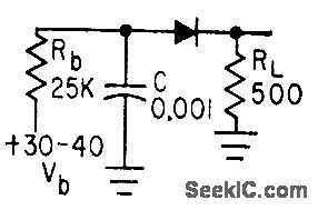
C discharges through negative-resistance diode and load after being charged by source, at rate determined by exponential function rather thon by RC time constant.-A. P. Schmid, Jr., Negative-Resistance Diode Handles High Power, Electronics, 34:34, p 44-46. (View)
View full Circuit Diagram | Comments | Reading(725)
CLASS_D_CB_NOISE_LIMITER
Published:2009/7/16 1:27:00 Author:Jessie

Two-step noise silencing system is almost essential for 27-Mc am receiver, because of ignition interference. large noise pulse swings plate of V3 negative and cuts off diode V3, to prevent noise pulse and audio signal from reaching volume control R3. Circuit recovers quickly, allowing audio signals to puss.-L. G.Sands, Citizens Radio Revision Spurs Equipment Design, Electronics, 32:15, p 55-57. (View)
View full Circuit Diagram | Comments | Reading(720)
SINE_SQUARE_WAVE_PHASE_SHIFT_OSCILLA_TOR
Published:2009/7/16 1:27:00 Author:Jessie

R1 controls oscillator frequency and R2 controls width of square wove having same frequency as sine-wave output.-F. W. Kear, Designing Transistor Phase-Shift Oscillators, Electronics, 35:11, p 72-74. (View)
View full Circuit Diagram | Comments | Reading(942)
AUDIO_DETECTOR_WITH_NOISE_LIMITER_2
Published:2009/7/16 1:26:00 Author:Jessie
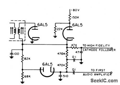
Uses shunt limiter in conjunction with series limiter, so noise pulses are prevented from operating agc circuit and thus desensitizing i-f amplifier of communication receiver.Broad-band cathode follower is connected to output of diode detector.-NBS, Handbook Preferred Circuits Navy Aeronautical Electronic Equipment, Vol. 1, Electron Tube Circuits, 1963, p N12-1. (View)
View full Circuit Diagram | Comments | Reading(826)
NEGATIVE_VOLTAGE_FROM_A_POSITIVE_SUPPLY
Published:2009/7/16 1:25:00 Author:Jessie

By using a 555 timer to generate a square wave and voltage-doubling the output, a negative voltage that is almost equal to the positive supply can be obtained. The current available is up to 20 to 30 mA or so, depending on the regulation and voltage needed. (View)
View full Circuit Diagram | Comments | Reading(1473)
| Pages:670/2234 At 20661662663664665666667668669670671672673674675676677678679680Under 20 |
Circuit Categories
power supply circuit
Amplifier Circuit
Basic Circuit
LED and Light Circuit
Sensor Circuit
Signal Processing
Electrical Equipment Circuit
Control Circuit
Remote Control Circuit
A/D-D/A Converter Circuit
Audio Circuit
Measuring and Test Circuit
Communication Circuit
Computer-Related Circuit
555 Circuit
Automotive Circuit
Repairing Circuit