Measuring and Test Circuit
DVM_CAPACITANCE_METER_ADAPTER
Published:2009/7/16 1:31:00 Author:Jessie | From:SeekIC

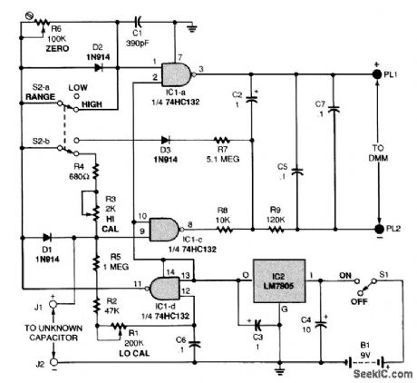
The figure shows the schematic for the capacitance meter adapter. When power switch S1 is in the ON position, an LM,7805 regulator (IC2) provides a 5-V source to the circuit. Switch 52 is used to select between the high- and low-capacitance ranges. The circuit measures from 0 to 2200 pF in its low range and from 0 to 2.2 μF in its high range. The adapter outputs 1 mV/pf in the lower range and 1 V/pF in the higher range. Those voltages would be displayed on a DMM, and would have to be read as capacitance values. Gate IC1-d is configured as a free-running oscillator whose frequency is determined by the setting of potentiometer R1. The output of IC1-d, pin 11, is a square-wave volt-age that is fed to the other two gates configured as inverters (IC1-a and IC1-c). A capacitor with an unknown value (CX) is connected across input terminals J1 and J2. Note that the positive lead of a polarized capacitor must be connected to J1. The capacitor under test charges through diode Dl on positive half cycles and discharges through R5 on negative half cycles in the low range, or through R3, R4, and R5 in the high range. In the high range, the square-wave output from IC1-d is fed directly to the inputs of the other two gates. With no capacitor connected to J1 and J2, the outputs of IC1-a and IC1-c are identical inverted versions of the input signal. The average voltage across the outputs of the gates at pins 3 and 8,In this case,is zero .With CX in place,and depending on its value,the input voltage to IC1-c,pin 9,stays higher longer than the input to IC1-a,pin 2.The output pulses from IC1-a and IC1-c are filtered and smoothed by R8,R9,C2,and C5 The average dc voltage across the outputs IS then proportional to the value of CX The circuit is a bit different in the low-range because compensation must be made for stray capacitance In the low range the output from IC1-d is fed to pin 1 of IC1-c through diode D2,which also charges C1 Capacitor C1 charges quickly and discharges slowly through potentiometer R6.The charge on C1 holds the input to IC1-a higher for a slightly longer time than would normally be the case That causes its inverted output to be low for a slightly longer time,and conversely high for a slightly shorter time Stray capacitance across input terminals J1 and J2 does the same thing to IC1-c,holding its input higher for a slightly longer time than would be the case f there were none Potentiometer R6 is adjusted so that the discharge time for C1 matches that of the stray capacitance and so cancels it out In the low range,an offset voltage is applied to the negative output terminal via D3,R7,and R8 to prevent the gates from locking together with such close trigger points
Reprinted Url Of This Article:
http://www.seekic.com/circuit_diagram/Measuring_and_Test_Circuit/DVM_CAPACITANCE_METER_ADAPTER.html
Print this Page | Comments | Reading(3)

Article Categories
power supply circuit
Amplifier Circuit
Basic Circuit
LED and Light Circuit
Sensor Circuit
Signal Processing
Electrical Equipment Circuit
Control Circuit
Remote Control Circuit
A/D-D/A Converter Circuit
Audio Circuit
Measuring and Test Circuit
Communication Circuit
Computer-Related Circuit
555 Circuit
Automotive Circuit
Repairing Circuit
Code: