
Circuit Diagram
Index 666
1_mA_CURRENT_SINK
Published:2009/7/16 1:48:00 Author:Jessie

A ftxed current flows through any load that is connected between the positive supply and Q1's collector. The noninverting terminal of the op amp is grounded, and negative feedback flows between the output of the circuit (Q1's emitter) and the inverting terminal. The voltage across R1 is thus equal to the voltage at the inverting terminal (approximately 0.55 V), so a fixed current of about 1 mA flows through the load, Q1's emitter, and R1.
(View)
View full Circuit Diagram | Comments | Reading(1154)
ULTRALINEAR_SWEEP
Published:2009/7/14 0:41:00 Author:May

Designed to generate horizontal and vertical sweep signals for military radar system, Linearity was so good that deviations could not be measured. With Ein positive as shown, circuit gives negative going sweep. Reverse input polarity to get positive-going sweep. Circuit is immune to short-circuits.-R. C. Scheerer, Designing Linear Sweep Generators, EDN|EEE Magazine, July 1, 1971, p 39-42. (View)
View full Circuit Diagram | Comments | Reading(943)
CAPACITIVE_SENSOR_SYSTEM
Published:2009/7/16 1:48:00 Author:Jessie
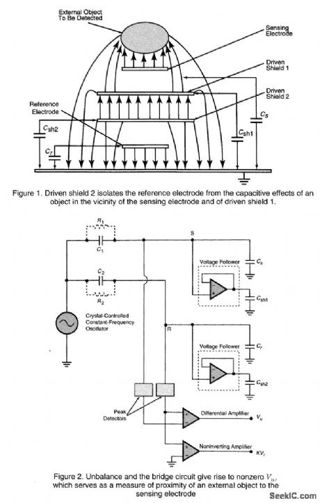


Figure1 illustrates the electric-field configuration of a capacitive proximity sensor of the capaciflector type. This one includes a sensing electrode driven by an alternating voltage, which gives rise to an electric field in the vicinity of the electrode; an object that enters the electric field can be detected by its effect on the capacitance between the sensing electrode and electrical ground. Also, it includes a shielding electrode (in this case, driven shield 1), which is excited via a voltage follower at the same voltage as that applied to the sensing electrode to concentrate more of the electric field outward from the sensing electrode, increasing the sensitivity and range of the sensor. Because the shielding electrode is driven via a voltage follower, it does not present a significant electrical load to the source of the alternating voltage. In this case, the layered electrode structure also includes a reference electrode adjacent to ground, plus a second shielding electrode (driven shield 2), which is ex-cited via a voltage follower at the same voltage as that applied to the reference electrode. Driven shield 2 isolates the reference electrode from the electric field generated by driven shield 1 and the sensing electrode, so a nearby object exerts no capacitive effect on the reference electrode. The excitation is supplied by a crystal-controlled oscillator and applied to the sensing and reference electrodes via a bridge circuit, as shown in Fig. 2. Fixed capacitors C1 and C2 (or, alternatively, fixed resistors R1 and R2) are chosen to balance the bridge-that is, to make the magnitude of the voltage at the sensing-electrode node,S equal the magnitude of the voltage at the reference-electrode node R. The voltages at, S and R are peak-detected and fed to a differential amplifier, which puts out voltage Vu=0. When an object intrudes, it changes Cs, unbalancing the bridge and causing Vu to differ from 0. The closer the object comes to the sensing electrode, the larger |Vu| becomes. An additional output voltage KVr is also available, where K is the amplification factor of a noninverting amplifier and Vr s the voltage on the reference electrode. (View)
View full Circuit Diagram | Comments | Reading(0)
RAMP_FROM
Published:2009/7/14 0:40:00 Author:May

10 V-Based on use of integrating opamp to generate triangle wave from square wave. Circuit goes one step further by convening triangle to ramp function having predetermined negative starting level of -10V. When square-wave input signal changes in polarity from positive to negative, output of circuit begins to go positive as ramp function and C4 charges with output voltage. When input changes from negative to positive and output begins to go negative, Q1 conducts and drives noninverting input of opamp negative. Since square-wave input is positive at this time, opamp output is forced to go negative at its slew rate. Output then remains negative until square-wave input switches in negative direction for repeating cycle.-L. Wing, Op Amp and One Transistor Produce Ramp Function, EDN Magazine, Nov. 15, 1972, p 49. (View)
View full Circuit Diagram | Comments | Reading(1138)
DIGITAL_RAMP_1
Published:2009/7/14 0:39:00 Author:May

RCA CD4004T IC, internally connected as ripple counter, provides flip-flop outputs corresponding to number of binary bits loaded into single input 1. Frequency range of counteris DC to 2.5 MHz, making it ideal for low-frequency operation. With R-2R ladder connected to flip-flop outputs, input square wave gives digitally stepped ramp at ladder output, with ramp frequency equal to 1/128 of input frequency.-W. E. Peterson, Digital Ramp Generator, EEEA Magazine, Jan. 1971, p 64-65. (View)
View full Circuit Diagram | Comments | Reading(928)
INVERTING_AMPLIFIER_GIVES_COMPLEMENT_OUTPUT
Published:2009/7/16 1:48:00 Author:Jessie

Only one transistor has isolated collector, so only three isolated lands are needed for integrated-circuit construction.-P. M. Thompson, Logic Principles for Multiemitter Transistors, Electronics, 36137, p 25-29. (View)
View full Circuit Diagram | Comments | Reading(469)
VARIABLE_START_STOP
Published:2009/7/14 0:37:00 Author:May

Ramp generator can be operated either in full ramp mode, with out-put sweeping from 0 to +10 V, or partial ramp mode in which output sweeps between adjustable starting point and adjustable stopping point. R5 selects time period in both modes. Ramp is reset automatically when output reaches preset voltage limit. Values shown for C2 and R5 give 100-s charge time, but changing R5 to 1 megohm increases charge period to 7 min. S3 stops ramp and resets circuit at any point in ramp cycle.-D. Dantuono, Ramp Generator Features Variable Start/Stop Points, EDN Magazine, April 20, 1978, p 130 and 132. (View)
View full Circuit Diagram | Comments | Reading(996)
NEON_TRANSISTOR_RELAXATION
Published:2009/7/16 1:47:00 Author:Jessie

Operates over range of 0.05 to 7,000 cps by adjusting values of C1, C2, and R4. Average supply current drawn is less than 1 ma.-R. D. Ryan, Low-Cost Pulse Generator, Electronics, 35:15, p 70. (View)
View full Circuit Diagram | Comments | Reading(606)
GATED_OSCILLATOR
Published:2009/7/16 1:47:00 Author:Jessie

Drives pair of pulse generators for selective calling system.-A. I. Perlin, Selective Calling for Data Link Systems, Electronics, 33:18, p 108-110. (View)
View full Circuit Diagram | Comments | Reading(1252)
107_MHz_SWEEP_GENERATOR
Published:2009/7/14 0:35:00 Author:May
Can be used with CRO for studying response of IF amplifier or filter. Greater dynamic range is obtained by using with spectrum analyzer-Circuits, 73 Magazine, Holiday issue 1976, p 170. (View)
View full Circuit Diagram | Comments | Reading(0)
POSITIVE_AND_NEGATIVE_VOLTAGE_POWER_SUPPLY
Published:2009/7/16 1:47:00 Author:Jessie

This circuit provides a precision voltage source that can be adjusted through zero to positive and nega-tive voltages, which eliminates reversing connections on the power supply. Also, it is possible to get exactly 0 V, without some offset.
As to how this circuit works, first consider the -1 V/V to + 1 V/V linear gain-control amp (see the figure). A Burr-Brown INA105 difference amp is used in a unity-gain inverting amp configuration. A potentiometer is connected between the input and ground.
The pot's slider is connected to the noninverting input of the unity-gain amp; this input is typically connected to ground. With the slider at the bottom of the pot, the circuit is a normal-precision unity-gain inverting amp witha gain of -1.0 V/V 10.01% maximum. Withthe slider at the top of the pot, the circuit is a normal-precision voltage follower with a gain of ±1.0 V/V ±0.001% maximum. With the slider in the center, there's equal positive and negative gain for a net gain of 0 V/V. The accuracy between the top and the bottom will usually be limited by the accuracy of the pot. (View)
View full Circuit Diagram | Comments | Reading(1115)
LIQUID_NITROGEN_LEVEL_CONTROL
Published:2009/7/14 0:35:00 Author:May

1N4005 diode serves as sensor. Junction voltage of diode increases from 0.7 V at room temperature to 1.05 V when in liquid nitrogen. Voltage change is used to activate amplifier that controls solenoid valve through solid-state relay.1K pot R adjusts circuit sensitivity; this can be set so pump starts refilling of container when liquid is as much as 2 inches below diode, to eliminate frequency recycling LED indicates valve status.-V.J.H. Chiu, Diode Sensor and Norton Amp Control Liquid-Nitrogen Level, Electronics, Feb.2,1978,p 117. (View)
View full Circuit Diagram | Comments | Reading(996)
MULTIEMITTER_TRANSISTOR_ALTERNATES_BETWEEN_AND_OR_LOGIC
Published:2009/7/16 1:47:00 Author:Jessie

Circuit performs and function first, then or function. For integrated-circuit construction, few isolated lands ore needed.-P. M. Thompson, Logic Principles for Multi-emitter Transistors, Electronics, 36:37, p 25-29. (View)
View full Circuit Diagram | Comments | Reading(471)
EXPONENTIAL_RAMP
Published:2009/7/14 0:34:00 Author:May

Used in curve tracer in which ramp does not need to be linear. Input romp output UJT Tr1 is Texas Instruments 43 or equivalent, ICs are SN72558P dual opamp or individual SN72741P opamps, and diodes are 1S44 or equivalent. Article gives other circuits and calibration procedure.-L.G. Guthbert, An F.E.T. Curve Tracer, Wireless World, April 1974, p 101-103. (View)
View full Circuit Diagram | Comments | Reading(867)
TANDEM_BRIDGE_FET
Published:2009/7/16 1:46:00 Author:Jessie

Provides tone bursts from 300-kc c-w input. Signal leakage in off condition is down 60 db.-F. J. Murphree and J. Bealor, FET in Bridge Circuit Gates a 300-KC Signal, Electronics, 38:9, p 60-61. (View)
View full Circuit Diagram | Comments | Reading(591)
DIGITAL_RAMP
Published:2009/7/14 0:33:00 Author:May

Digiial-to-analog technique using single CD4024A CMOS shift register eliminates temperature and linearity problems normally encountered when using RC circuit to drive VCO of digital ramp. Ramp is generated from 50-kHz clock and stopped by applying reset pulse to counters, Use of stable but variable supply for IC permits adjustment of ramp output amplitude, Ramp itself consists of large number of small steps; if these steps are too large, second CD4024A can be added and clock frequency increased. If response of 741 opamp is not adequate for very steep ramps, use opamp having higher slew rate.-K. Bower, CMOS Linear-Ramp Generator Has Amplitude Control, EDN Magazine, June 20, 1973, p 87. (View)
View full Circuit Diagram | Comments | Reading(1820)
TUNNEL_DIODE_OR_CIRCUIT_AND_ENVELOPE_GENERATOR
Published:2009/7/16 1:45:00 Author:Jessie

Used as part of program pulse generator incorporating ring of four stages, diode-matrixed with ring of three stages to provide twelve-bit words at 30-Mc dock rate.C6 and R2 are a-c terminations for coax from output of ring counter.-W. V. Harrison and R. S. Foote, funnel Diodes Increase Digital-Circuit Switching Speeds, Electronics, 34:32, p 154.-156. (View)
View full Circuit Diagram | Comments | Reading(572)
VOLTAGE_CONTROLLE_D_RAMP
Published:2009/7/14 0:31:00 Author:May

Current source Q1 and C1 together set duration time of ramp. As positive DC voltage at gate of MPU131 is increased, peak point firing voltage of PUT is changed and duration time is increased. With 0.01μF, control voltage change from 5 V to 20 V increases duration time linearly from 2 ms to 7.2 ms.-R. J. Haver and B. C. Shiner, Theory, Characteristics and Applications of the Programmable Unijunction Transistor, Motorola, Phoenix, AZ, 1974, AN-527, p 8. (View)
View full Circuit Diagram | Comments | Reading(697)
SΥNCHRONOUS_SWITCH
Published:2009/7/14 0:30:00 Author:May

Mullard TCA280A trigger module provides triggering of load triac at zero crossings of AC line voltage. Values shown are for triac requiring gate current of 100mA; for other triacs, values of Rd, Rg, and C1 may need to be changed. Designed for resistive loads and ON/OFF rather than propoltional control.- TCA280A Trigger IC for Thyristors and Triacs, Mullard, London, 1975, Technical Note 19, TP1490, p 10. (View)
View full Circuit Diagram | Comments | Reading(1128)
1000_V_PULSES
Published:2009/7/16 1:45:00 Author:Jessie

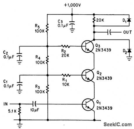
Positive 3-v input pulse switches Q1, Q2, and Q3 on in sequence, to produce l,000-v pulse with short rise time for driving 20-kv pulse tube. High-voltage rectifier diodes protect transistor string from spurious high-voltage spikes.-D. O. Hansen, Transistor Circuit Pulses l,000 Volts, Electronics, 38:18, p 86. (View)
View full Circuit Diagram | Comments | Reading(1036)
| Pages:666/2234 At 20661662663664665666667668669670671672673674675676677678679680Under 20 |
Circuit Categories
power supply circuit
Amplifier Circuit
Basic Circuit
LED and Light Circuit
Sensor Circuit
Signal Processing
Electrical Equipment Circuit
Control Circuit
Remote Control Circuit
A/D-D/A Converter Circuit
Audio Circuit
Measuring and Test Circuit
Communication Circuit
Computer-Related Circuit
555 Circuit
Automotive Circuit
Repairing Circuit