
Circuit Diagram
Index 663
VOICE_ACTIVATED_TAPE_RECORDER_SWITCH
Published:2009/7/14 1:27:00 Author:May

A schematic of the tape recorder switch is shown The circuit can be powered by B1, which is four AA batteries in series or any 6-Vdc supply. Audio signals from the electret Microphone,MIC1,are coupled via capacitor C1 to two audio-amplification stages centered around transistors Q1 and Q2 A 5000-Ω Potentiometer, R12,provides a sensitivity control that sets the audio level at which the switch will activate a tape recorder The audio input to the digital switching section of the circuit is biased at half the supply voltage by two 1-percent,1-MΩ,metal-film resistors (R6 and R7) Integrated Circuit U1 is a 74HC14 hex Schmitt-trigger inverter. With a 6-V power supply,the Schmitt inverter gates will have a l-V hysteresis gap between 2.2 and 3.2 V That means that the input to a Schmitt inverter must rise above 3.2V for the output to go low; but must fall below 2.2V for the output to return to a high,The low on pin 3 of U1-b in the Presence of audio is presented to pin 11 of U1-e and ends up at pin 8 of U1-d That will pull pin 1 low in the absence of an audio signal from the microphone,making pin 2 high Diode D2 blocks the discharging of C5 through its original charging path, so C5 starts to discharge through R9. After that delay, the voltage at pin 3 rises above 3.2 V, thus removing the connection from terminal A to ground and turning off the tape recorder. A continuous audio input to pin 1 will hold pin 4 high, but soon as it ceases, the time-out process begins. When power is applied to the circuit using switch S2, LED1 lights. However, if the ground connection to R11 is removed, and that end of the resistor is then connected to terminal X (pin 6 of U1-c), the LED will instead light only when the output of the circuit is active. (View)
View full Circuit Diagram | Comments | Reading(1539)
CURRENT_ECONOMIZING_DESIGN
Published:2009/7/14 1:26:00 Author:May

Used in 15-stctge counter. Circuit is conventional, but to economize on current, only first three stages operate with relatively high collector currents; for these, RI and R2 +R3 are 5,600 ohms and transistors are 2N496. Subsequent stages use OC201 transistors and increasingly higher values of collector load, up to 22,000 ohms for 8th stage.-J. Ackroyd, Orbiting Spectrometer Plots Solar X-Rays, Electronics, 34:43, p 55-57. (View)
View full Circuit Diagram | Comments | Reading(650)
BATTERY_SIMULATOR_CIRCUIT
Published:2009/7/14 1:26:00 Author:May

When developing a battery charger, using a real battery might be inconvenient. The battery simulator circuit described here is an alternative. The battery input positive and negative terminals should be connected in place of the battery in the charger circuit. Also, a current-limited lab-type power supply must be connected to the simulator circuit (as shown). In Discharge mode, the battery simulator uses the current-limited lab power supply PS1 as a source, and the simulator is inactive. In Charge mode, charge current is forced through the battery input terminals. Low voltage that develops across R8 is amplified by U1 and causes Q1 to shunt the charge current while maintaining the power-supply (PS1) voltage. U2, L1, CR2, C3, and C4 produce an internal 12-V power supply that is required to operate U1 and drive Q1. The PS1 voltage range is 1.5 to 15 V. Diode CR1 protects the circuit from reverse polarity and is needed if the maximum charge current is too high for the body diode of Q1 (Q1 must be heat sunk). R1 is a sense resistor for measuring the charge current. R10 and C5 simulate the ac characteristics of the battery. (View)
View full Circuit Diagram | Comments | Reading(3253)
MEASURING_PEAK_POWER
Published:2009/7/14 1:26:00 Author:May

Addition of amplifier and rectifier circuits to Heath HM-102 or other similar RF wattmeter permits measurement of transmitter peak power output. DPDT toggle switch S2 is added to wattmeter to give choice of measurement desired. Circuit uses LM1458 or equivalent dual opamp. Current passing through 1N914 diode charges 0.1-μF capacitor at pin 3 of U1A, delaying meter return to zero long enough for reading of peak. When pointer just starts moving downward, next spoken word kicks it back up to peak value. To calibrate, set 10K pot so peak reading (S2 at PEP) is equal to normal reading (S2 at NORMAL) while using CW output of transmitter as test signal. CR1 is 2-A 50-PlV bridge rectifier. T1 has 12.6.V center-tap 100-mA secondary.-G. D. Rice, PEP Wattmeter-a la Heath, QST, Dee. 1976, p 30-3t. (View)
View full Circuit Diagram | Comments | Reading(3165)
BUFFER
Published:2009/7/14 1:25:00 Author:May
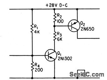
Used between ring counters when readout number has several digits, to make final stage of one counter fire first stage of next counter while resetting first counter.-F. W. Kear, Digital Control Uses Unijunction Transistors, Electronics, 34:18, p 79-80. (View)
View full Circuit Diagram | Comments | Reading(794)
7_W_FOR_QRP
Published:2009/7/14 1:24:00 Author:May

Operates at 7-W peak power for outing through interference when operating on low power on any CW band from 80 to 10 meters with typical inefficient antenna systems of portable operation, Q1 is 2N709 VFO feeding 2N697 amplifier a3 through 2N697 buffer Q2. Q4 is GE63 driver for Motorola HEP53001 final amplifier Q5. Keying can be introduced at Q2, Q3, or Q4. Article gives coil-winding data for all bands and covers construction and operation in detail. -J. Huffman, The Mini-Mite Allband QRP Rig, 73Magazine, Jury 1976, p 30-32 and 34-35. (View)
View full Circuit Diagram | Comments | Reading(693)
LOGICALLY_REDUNDANT_INVERTER
Published:2009/7/15 22:32:00 Author:Jessie

Symmetrical design with series-based diodes makes inverter independent of any single component failure.-T. Golstein, Reliable Circuits Through Redundancy, EEE, 11;3, p 56-59. (View)
View full Circuit Diagram | Comments | Reading(592)
FUNCTION_GENERATOR_POWER_BUFFER
Published:2009/7/14 1:18:00 Author:May

This buffer circuit can be used as an output booster for any function generator that has to be extended in order to drive several loads. The heart of the circuit is a video distribution amplifier IC from Elantec, the EL2099CT (listed by RS Components). This interesting device has a 3-dB power bandwidth of no less than 65 MHz at a gain of x2. Here, it is used to drive up to four 50-Ω loads at a maximum signal level in excess of 10 Vpeak. When used for video applications, the EL2099CT can drive up to six 75-Ω loads. The gain of the amplifier is x2; unity gain is not possible because of instability problems. The bandwidth of the circuit shown here is >10 MHz, while the output achieves a drive margin of >10 Vpeak . Current consumption will be of the order of 200 mA. (View)
View full Circuit Diagram | Comments | Reading(5040)
VARIABLE_WIDTH_AND_DELAΥ
Published:2009/7/15 22:31:00 Author:Jessie
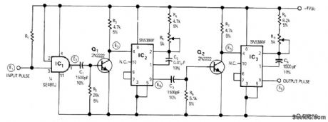
Produces variable-width blanking pulse at selectable delay time after triggering by input pulse. With values shown, output pulse range is 8 to 12 μs, and delay range is independently adjustable from 26 to 36 μs with R5.-D. E. Norris, Variable Delay Blanking-Pulse Generator, EDN|EEE Magazine, Dec. 1, 1971, p 49. (View)
View full Circuit Diagram | Comments | Reading(768)
LED_BATTERY_MONITOR_FOR_12_V_STSTEMS
Published:2009/7/14 1:18:00 Author:May

This monitor is handy in cars and is particularly suitable for radio amateurs who power their equipment from a car battery. Bridge rectifier D9-D12 ensures that the battery cannot be connected with incorrect polarity. The zener voltage of diodes D5-D8 increases in standard steps, so the battery voltage needs to be higher to cause successive LEDs to light. In other words, the higher the battery voltage, the more LEDs will light. The component values are chosen so that at a battery voltage of 9 V-battery poor-only D1 lights; when it is about 11 V-battery doubtful-D1 and D2 light; when it is 13 V-battery fine-D1, D2, and D3 light. Diode D4 is a flashing LED. The value of zener diode D8 is such that the LED begins to flash when the battery voltage approaches 15 V-that is, an overvoltage situation. (View)
View full Circuit Diagram | Comments | Reading(2175)
LIGHT_BLOCK_SENSOR
Published:2009/7/15 22:30:00 Author:Jessie

In this circuit, relay RY1 remains open until the light source is blocked. As long as the IR light source is uninterrupted, phototransistor Q1's collector voltage is near zero. The voltage at zener diode D2's cathode is too low for conduction, keeping transistor Q2 off and the RY1 open. (View)
View full Circuit Diagram | Comments | Reading(1648)
SHORTENING_DUTY_CYCLE
Published:2009/7/15 22:30:00 Author:Jessie
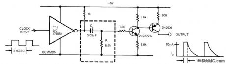
Clock-pulse differentiator/buffer shortens duty cycle of 500-Hz clock signal having positive period of 1000 ps. Open-collector 7405 inverter acts as buffer. Ct and Rt are primary differentiating components.Saturation of transistors provides some stretching of output and gives output pulse width of about 180 μs. Developed for driving regulated power supply having clock-controlled short-circuit protection.-J. L. Bohan, Clocking Scheme Improves Power Supply Short. Circuit Protection, EDN Magazine, Match 5, 1974, p 49-52.
(View)
View full Circuit Diagram | Comments | Reading(614)
TRICOLOR_LED_NiCd_CHECKER
Published:2009/7/14 1:14:00 Author:May
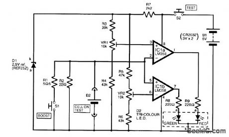
This circuit uses a window comparator and a bicolor LED. VR1 and VR2 set the high and low trip points of the comparators, respectively. The LED shows green for highest voltage (good), yellow for intermediate, and red for low voltage (bad). The circuit can be calibrated for other voltages and is generally useful as a voltage indicator. (View)
View full Circuit Diagram | Comments | Reading(2700)
LAGHT_ACTIVATED_SWITCH
Published:2009/7/15 22:28:00 Author:Jessie

When even a little light hits light-dependent resistor R5, transistor Q1 is turned off because the base has less resistance to the ground than to the positive rail. In that situation, the base is at a negative potential. When the sun sets, R5 is no longer illuminated, giving the transistor's base a high resistance to ground-higher than 100,000Ω. With less resistance to positive potential, the base is biased, turning on Q1. Relay RY1 is then energized and pulls in, connecting the SCR1's anode to positive potential. The 555 timer, IC1, powers up, and its output goes high to approximately 10.67V, which is sufficient to energize RY2. Relay RY2 then pulls in, keeping the ac bulb on the whole night, and turning it off again at sunrise. (View)
View full Circuit Diagram | Comments | Reading(867)
MAX038_FUNCTION_GENERATOR_1
Published:2009/7/14 1:11:00 Author:May
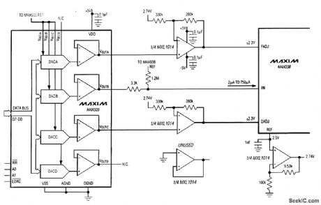
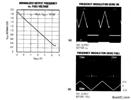
To adjust the frequency digitally, connect a voltage-output DAC to ⅡN via a series resistor, as shown. The converter output ranges from 0 V at zero to 2.5(255/256) V at full scale. Current injected by the converter into ⅡN, therefore, ranges from 0 to 748 μA. The 2.5-V reference and 1.2-Ω resistor inject a constant 2μA, so (by superposition) the net current into ⅡN ranges from 2 μA (at a code of 00000000) to 750μA (at 1111 1111). The quad DAC IC operates from 5 V or ±5 V. As described below, it can also provide digital control of FADJ and DADJ. For fine adjustments (±70 percent), apply a control voltage in the range ±2.3 V to the frequency adjust (FADJ) terminal. Both FADJ and ⅡN have wide bandwidths that allow the output frequency to be modulated at a maximum rate of about 2 MHz. As the more linear input, ⅡN is preferred for open-loop frequency use in a phase-locked loop. For digital control of FADJ, conftgure a DAC and external op amp (as shown in the figure) to produce an output ranging from -2.3 V (00000000) to 2.3 V (1111 1111). (View)
View full Circuit Diagram | Comments | Reading(958)
01_999_DUTY_CYCLE
Published:2009/7/15 22:28:00 Author:Jessie
Single opamp circuit provides precise duty-cycle control of pulse train over wide dynamic range by choice of values for R1 and R2. Opamp forms gain element of astable MVBR, with pulse and space time intervals determined by feedback elements. Values shown give duty-cycle ratio of 0.001 and period of 1 s. J. Graeme, Pulse Generator Offers Wide Range of Duty Cycles, EDN|EEE Magazine, Sept.1, 1971, p 42-43. (View)
View full Circuit Diagram | Comments | Reading(913)
GROUND_REFERENCED_RAMP_AND_PEDESTAL_CONTROL
Published:2009/7/14 1:08:00 Author:May

Need for transformer is eliminated by applying alternate half-cycles to inverting and noninverting inputs of section 3 of LM3900 quad opamp, so full-wave-rectified waveform is referenced to ground. Comparator opamp 1 discharges timing capacitor at zero line voltage and synchronizes circuit with line frequency. Buffer opamp 2 scales input and provides linear pedestal for capacitor. Opamp 4 is comparator serving as output driver whose output is high when capacitor is charged to level selected by high-end trimming pot. Output is sufficient for optoisolators and logic triacs.-J.C. Johnson, Ramp-And-Pedestal Phase Control Uses Quad Op Amp, EDN Magazine, June 5, 1977, p 208 and 211. (View)
View full Circuit Diagram | Comments | Reading(1050)
LOSS_OF_LIGHT_DETECTOR
Published:2009/7/15 22:26:00 Author:Jessie

Light falling on Q1 causes Q1 to conduct. When the light fails, C1 charges toward +9V, triggering SCR1, lighting LED1. S1 resets the SCR. (View)
View full Circuit Diagram | Comments | Reading(775)
80_VRMS_ANALOG_SWITCH
Published:2009/7/14 1:07:00 Author:May

Developed for switching high-level analog signals with speed, accuracy, and reliability, for such applications as digital-to-synchro converters. Feedback net-work stabilizes output against changes in circuit parameters. For AC signal inputs between±10 V, -12 VDC on gate of FET blocks input channel and R2 grounds inverting input of opamp A1 to prevent noise pickup and minimize voltage offset. Grounding gate of FET turns on input channel;input signal is then amplified by A1 and fed to unity-gain power opamp A2.-D.J. Musto, Analog Switch and IC Amp Controls 80V RMS, EDN Magazine, Feb 20, 1973, p 91-92. (View)
View full Circuit Diagram | Comments | Reading(888)
_10_V_WITH_BOOTSTRAPPED_OPAMP
Published:2009/7/15 22:24:00 Author:Jessie

High-stability Precision Monolithics 0P-07A bipolar-input opamp with ultralow offset voltage provides precise 10 V virtually independent of changes in supply voltage, ambient temperature, and output loading. Choose value of R1 to maintain zener current at exactly 2 mA, using 5 PPM/'C resistor. All resistor values are determined from exact zener voltage Vz, as given by equations alongside circuit.-D. Soderquist and G. Erdi, The OP-07 Ultra-Low Offset Volt-age 0p Amp-a Bipolar Op Amp That Challenges Choppers, Eliminates Nulling, Precision Monolithics, Santa Clara, CA, 1975, AN-13, p 8 (View)
View full Circuit Diagram | Comments | Reading(777)
| Pages:663/2234 At 20661662663664665666667668669670671672673674675676677678679680Under 20 |
Circuit Categories
power supply circuit
Amplifier Circuit
Basic Circuit
LED and Light Circuit
Sensor Circuit
Signal Processing
Electrical Equipment Circuit
Control Circuit
Remote Control Circuit
A/D-D/A Converter Circuit
Audio Circuit
Measuring and Test Circuit
Communication Circuit
Computer-Related Circuit
555 Circuit
Automotive Circuit
Repairing Circuit