
Circuit Diagram
Index 676
BIQUINARY_COUNTER_WITH_READOUT
Published:2009/7/13 22:13:00 Author:May
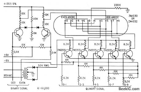
Simplified driver circuits require only seven transistor rather ten, when used with special Amperex ZMl032 tube.-Biquinary Indicator Uses 7 Transistors, Electronics, 36:28, p58.
(View)
View full Circuit Diagram | Comments | Reading(907)
125_ns_POWER_SWITCH
Published:2009/7/13 22:13:00 Author:May

Developed for repetitive pulse applications in which rise, fall, and storage times of pulse must be kept at absolute minimum. Circuit provides very high gain of Unitrode U2T601 Darlington and switching speeds up to 5 times greater than conventional techniques. Load power up to 10 A is typically applied within 125 ns. Applications include drive for laser diode and for radar circuits.- Designer's Guide to Power Darlingtons as Switching Devices, Unitrode, Watertown, MA, 1975, U-70, p 19. (View)
View full Circuit Diagram | Comments | Reading(642)
CLIPPING_OPAMP
Published:2009/7/13 22:13:00 Author:May

Simple circuit limits excursion of DC input voltage to level precisely equal to DC reference input voltage. When referenceis 0 V, circuit can be used as half-wave rectifier up to 100 kHz. Feedback overcomes breakover characteristics of D2, to provide sharp clipping at levels from mitlivolts to volts. At 10 kHz, with D1 omitted, range of levels is 70 mVRMS to 7 VRMS. With D1, circuit is useful at levels down to 0.3 VRMS at 100 kHz.-R. S. Burwen, Precision Clipper Operates from Millivolts to Volts, EDN Magazine, Dec. 1, 1972, p 57 and 59. (View)
View full Circuit Diagram | Comments | Reading(850)
SIMPLE_SAWTOOTH_WAVEFORM_GENERATOR
Published:2009/7/13 22:12:00 Author:May

This sawtooth generator is built around a 555 configured as an astable multivibrator. (View)
View full Circuit Diagram | Comments | Reading(1023)
BINARY_WITH_STEERING_CIRCUIT_TRANSISTOR
Published:2009/7/13 22:12:00 Author:May
Input goes to steering transistor that replaces two back-to-back diodes normally used to drive bases of binary transistors through capacitive coupling. For-transistor binary flip-flop reduces total quiescent drain on batteries.-R.W. Rochelle. Cyclops Cores Simplify Earth-Satellite Circuits. Electronics.31:9,p56-63. (View)
View full Circuit Diagram | Comments | Reading(1447)
MODEL_ROCKET_IGNITION_CIRCUIT
Published:2009/7/13 22:10:00 Author:May
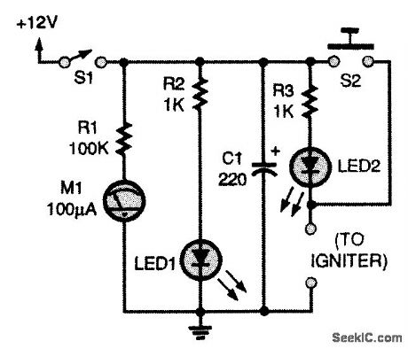
This circuit requires a 12-Vdc source. A battery pack of eight AA cells in series will work. Meter M1 gives you an indication of battery voltage; change the batteries when you see a noticeable drop in current. The circuit contains two LEDs: LED1 reminds you that the circuit is powered up, and LED2 lets you know that you have continuity through the igniter and are ready to fly. Capacitor C1 gives igniters that extra kick they occasionally need. Pushing the momentary push-button switch (S2) sends the rocket on its way. Use a red switch for that. The igniter leads are connected to the plugs marked igniter. (View)
View full Circuit Diagram | Comments | Reading(1078)
TIME_DELAYED_MODEL_ROCKET_LAUNCH_CONTROL
Published:2009/7/13 22:07:00 Author:May

The circuit, which gives a choice of six delay settings, consists of three 555 oscillator/timers (U1 to U3), a pair of transistors (Q1 and Q2), four switches (S1 to S4), a piezoelectric buzzer (BZ1), and a few support components. Power for both the control circuit and the rocket-engine igniter is provided by a 6-V power source that is composed of four AA-cell alkaline batteries. Closing switch S1 feeds power to the launch-control circuit, but does not initiate a launch sequence. A pair of series RC circuits(R4-C9 and R8-C12, respectively) are used to debounce the RESET inputs (pins 4) of U1 and U2 (a pair of 555 oscillator/timer ICs). When S2 is closed, C1's negative terminal is connected to ground through the switch, momentarily pulling pin 2 of U1 (which is configured as a monostable multivibrator, or one-shot) low, activating it. Once triggered, U1's output goes high for an interval that is determined by R3 and one of six timing capacitors (C2 through C8). The timing capacitor is selected via DELAY SELECTOR switch S3. The high output of U1 at pin 3 causes Q2 to turn on, allowing the piezoelectric buzzer BZ1 to turn on. Monostable U1's output is also fed to the RESET input of U3 at pin 4, causing it to oscillate with a duty cycle of about 75 percent. As long as the output of U1 is high and the astable is oscillating, BZ1 beeps once every 4 s. The resistor discharges coupling capacitor C10 whenever U1's output goes high. At the end of the selected time delay, U1's output goes low.That low is coupled through C10 and D1 to the TRIGGER input (pin 2) of U2. Components R7 and C11 set U2's high-output interval to approximately 3 s. During that 3-s interval, U2's high output at pin 3 is fed to Darlington transistor Q1 through R9. With S4 in the LAUNCH position, Q1 grounds one end of the engine igniter, effectively connecting it to the battery's negative terminal. (View)
View full Circuit Diagram | Comments | Reading(3396)
4224_MHz_CRYSTAL_OSCILLATOR
Published:2009/7/13 22:05:00 Author:May

Uses 105.6-MHz crystal oscillator followed by frequency-doubling stages to give desired output for driving external diode-type tripler for which circuit is also given in article, Developed for use in 1296-MHz SSB transceiver for 23-cm amateur band.-H. P. Shuch, Easy-to-Build SSB Transceiver for 1296 MHz, Ham Radio, Sept. 1974, p 8-23. (View)
View full Circuit Diagram | Comments | Reading(1831)
LINE_VOLTAGE_COMPENSATION
Published:2009/7/13 22:05:00 Author:May

Can be used with either half-wave or full-wave phase control circuit to make load voltage independent of changes in AC line voltage.P1 is adjusted to provide reasonably constant output over desired range of line voltage. As line voltage increases, P1 wiper voltage increases. This has effect of charging CT to higher voltage so more time is taken to tagger UJT. Additional delay reduces thyristor conduction angle and thereby maintains desired average voltage.-D.A. Zinder, Unijunction Trigger Circuits for Gated Thyristors, Motorola, Phoenix, AZ, 1974, AN-413, p 4. (View)
View full Circuit Diagram | Comments | Reading(712)
SELF_BUFFERED_SERIES_CLIPPER
Published:2009/7/13 22:04:00 Author:May

Provides negative clipping of sine.wave input, using 2620 opamps with diodes as linear OR gate. When input voltage is greater than reference voltage, A1-D1 turns on and input voltage appears at output. When Ein falls below Vref, A2-D2 provide Vref as output signal. With 2620, circuit gives good performance to above 10 kHz. For positive clipping, reverse diode connections and return R1 to +15 V. Circuit provides low output impedance.-W. G, Jung, IC Op-Amp Cookbook, Howard W. Sams, Indianapolis, IN, 1974, p 187-189. (View)
View full Circuit Diagram | Comments | Reading(633)
ALL_CHANNEL_VFO_FOR_2_METERS
Published:2009/7/13 22:04:00 Author:May
Permits coverage of all channels with ordinary FM transceiver without costly frequency synthesizer or individual channel crystals. Can also be used for tuning input of repeater when made necessary by malicious or accidental interference. Replaces first crystal oscillator in FM transceiver and tunes over required range, generally onethird of first injection frequency. Operates at about 45 MHz for most transceivers, but frequency can easily be changed. Tuning pot (10-turn 5K with digital dial is best) can be placed remotely. VFO uses FET oscillator tuned by tuning diode (also known as Varicap, varactor, or variable-capacitance diode). Source-follower output stage buffers oscillator. Supply is regulated by zener. Q1 and Q2 can be MPF102 FETs, but 2N5668 or 2N5669 are better. L1 is 4 turns No. 16 1/2 inch in diameter. Article covers construction, testing, and installation in transceiver.-P. Franson, Simple Tunable Receiver Modification for VHF FM, Ham Radio, Oct. 1974, p 40-43. (View)
View full Circuit Diagram | Comments | Reading(1117)
FULL_WAVE_AC_CONTROL
Published:2009/7/13 22:04:00 Author:May

Motorola type MDA920-1 bridge rectifier provides full-wave rectification of AC line voltage for 2N5064 SCR placed across DC output of bridge. When positive logic pulse from CMOS circuit energizes optoisolator, SCB conducts and completes path for triac gate trigger current through bridge and SCR, turning on AC load. Triac rating determines size of load. Drawback of circuit is generation of EMI if logic signal occurs at other than zero crossings of AC line.-A. Pshaenich, Interface Techniques Between Industrial Logic and Power Devices, Motorola, Phoenix, AZ, 1975, AN-712A, p 17. (View)
View full Circuit Diagram | Comments | Reading(1593)
6545_6845_MHz_VFO
Published:2009/7/13 22:03:00 Author:May

Covers 40-meter amateur band of transceiver for SSB and CW with stable incremental tuning circuit using Motorola MV1654 varactor diode CR3. Tuner permits up to 10-kHz offset above or below VFO frequency. Varactor control voltage is set by offset tuning control R3. R4 compensates for differences in varactors and adjusts VFO for zero off-set. Output buffering is provided by Q6 and Q7, with 07 also serving as power amplifier for balanced mixer used in companion exciter of transmitter. S2 activates receiver offset. Relay K1 automatically turns off offset when receiver is in transmit or standby mode, Offset feature is needed only if there is frequency difference between transmitted and received signals. L4 has 5 turns No. 22 on 1/2-inch slug-tuned ceramic form.-W. J. Weiser, Simple SSB Transmitter and Receiver for 40 Meters, Ham Radio, March 1974, p 6-20. (View)
View full Circuit Diagram | Comments | Reading(2080)
10_CHANNEL_MULTIPLEXER
Published:2009/7/13 22:02:00 Author:May

Basic counter consists of ten modified bistable mvbr stages, Q1 through Q20, coupled in usual ring manner and driven continuously by timing oscillator Q31. Used for multiplexing conventional or random pulse inputs from Explorer VII satellite. Eight channels serve for information inputs, and fixed levels of 0 and 110% are applied to other two channels for frame identification.-O. B. King, Multiplexing Techniques for Satellite Applications, Electronics, 32:44, p 58-62. (View)
View full Circuit Diagram | Comments | Reading(697)
LOW_VOLTAGE_BATTERY_SWITCHOVER_SYSTEM
Published:2009/7/13 22:00:00 Author:May

Portable systems often include the flexibility to operate either from an internal battery or from an ac-dc wall adapter. Many such systems include circuitry that switches automatically between an internal battery and an external source as the user connects and disconnects the wall adapter. The circuit shown implements this idea with a dual linear regulator, one side of which is preset for a regulated output of 2.84 V.(other versions of the IC offer 2.80-V and 3.15-V outputs). The other side of the regulator id configured to allow user-adjustable outputs, but, in this case, it monitors the wall-adapter voltage. When that voltage is removed by unplugging the adapter, the regulator's pass transistor routes battery current into the IC for support of the 2.84-V output (current flow in this transistor is counter to that of most applications). The input bypass capacitor (C1) provides enough holdup time for seamless transitions between the battery and adapter voltages. Resistors RI and R2 sense the wall-adapter voltage and determine the switchover threshold, 'VSW VSW = Vset【(R1+R2)/R2】 = 1.25V【(130kΩ+100kΩ)/100kΩ】 = 2.875vDiode Dl isolates the wall-adapter voltage so that the battery can't cause limit cycling by retriggering the switchover. D2 holds the IC's dual-mode input in the external feedback mode by maintaining a minimum voltage at the SET2 input. The wall-adapter voltage should be equal to or greater than the maximum battery voltage. (View)
View full Circuit Diagram | Comments | Reading(759)
SYMMETRICAL_BIOPLAR
Published:2009/7/13 21:59:00 Author:May

Circuit uses transistor feedback, with cument returned to opamp summing point through emitter-followers Q1 and Q2. When output E0 rises to positive voltage high enough so tap on R4, makes Q1 turn on, output of A1 is limited to value corresponding to setting of R4. Q2 performs similar limiting function for negative swings of input signal. R4 sets limiting level for both polarities, for variable symmetrical limiting. Transistors and opamps shown are selected for high-speed operation.For single-polarity limiting, insert large resistance RB in base lead of remaining transistor to prevent it from conducting heavily on output voltage swings.-W. G. Jung, IC Op-Amp Cookbook, Howard W. Sams, Indianapolis, IN, 1974, p 203-204.
(View)
View full Circuit Diagram | Comments | Reading(590)
FAST_SWITCHING_TTL_INTERFACE_FOR_VMOS
Published:2009/7/13 21:59:00 Author:May

Totem-pole TTL interface drive for S55V01 VMOS gives appreciably faster switching times (less than 30 ns). To achieve fast turn-on time without unduly small pull-up resistor, which dissipates considerable power when switch is in OFF state, emitter-follower Q1 drives high peak currents into capacitive VMOS input.-L. Shaeffet, VMOS Peripheral Drivers Solve High Power Load Interface Problems, Computer Design, Dec. 1977, p 90, 94, and 96-98. (View)
View full Circuit Diagram | Comments | Reading(812)
ROCKET_LAUNCHER_VOICE_COUNTDOWN_RECORDER_CIRCUIT
Published:2009/7/13 21:57:00 Author:May

Use this circuit to record your countdown sequence on the ISD1000A. Once you are satisfied with your recording, the circuit will no longer be needed.This circuit can be used as a stand-alone voice recorder circuit. (View)
View full Circuit Diagram | Comments | Reading(4433)
SWITCHING_4500_W_AT_UP_TO_10_kHz
Published:2009/7/13 21:56:00 Author:May

Darlington connection of Delco DTS-709 transistors will switch 7 A at 700 V with 1-μs switching time. Suitable for motor speed control,switching regulator、and inverter applications. Can be operated directly from 440-VAC line. Q1 and Q2 are 2N6100. Diodes are 1N4001 C1 is 4 μF at 15V. R1 is 510 ohms,R2 is 100, R3 is 12,R4 is l0, R5 is 1K, R6 is 47 and R7 is 100,- Low Cost'Duolithic Darlington'Switches 4500 Watts at up to 10 kHz, Delco, Kokomo,IN,1973, Application Note 54,p 2. (View)
View full Circuit Diagram | Comments | Reading(846)
MULTIJUNCTION_SEMICONDUCTOR_AS_DECADE_COUNTER
Published:2009/7/13 21:56:00 Author:May
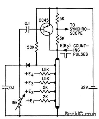
Experimental equivalent of cold-cathode counter tube, developed in Poland, cam serve also as staircase wave form generator. Although circuit shown, with five gm junctions on one side of n-type semi-conductor bur, gives only count of five before transistor restores initial state, decade counter would have ten junctions on bar.-A. Ambroziak, Semiconductor Analog of a Cold-Cathode Counter Tube, Electronics, 35:6, p 46-47. (View)
View full Circuit Diagram | Comments | Reading(1118)
| Pages:676/2234 At 20661662663664665666667668669670671672673674675676677678679680Under 20 |
Circuit Categories
power supply circuit
Amplifier Circuit
Basic Circuit
LED and Light Circuit
Sensor Circuit
Signal Processing
Electrical Equipment Circuit
Control Circuit
Remote Control Circuit
A/D-D/A Converter Circuit
Audio Circuit
Measuring and Test Circuit
Communication Circuit
Computer-Related Circuit
555 Circuit
Automotive Circuit
Repairing Circuit