
Circuit Diagram
Index 677
HIGH_SPEED_BUFFERED_FLIP_FLOP
Published:2009/7/13 21:56:00 Author:May


Buffering increases load-handling capacity and insures accurate counting of 10-Mc clock frequencies.-D. L. Nepveux , Digital Circuits Achieve Automatic Control of Radar Range Tracking, Electronics, 34:52, p 46-50. (View)
View full Circuit Diagram | Comments | Reading(577)
MAX038_FUNCTION_GENERATOR_
Published:2009/7/13 21:53:00 Author:May
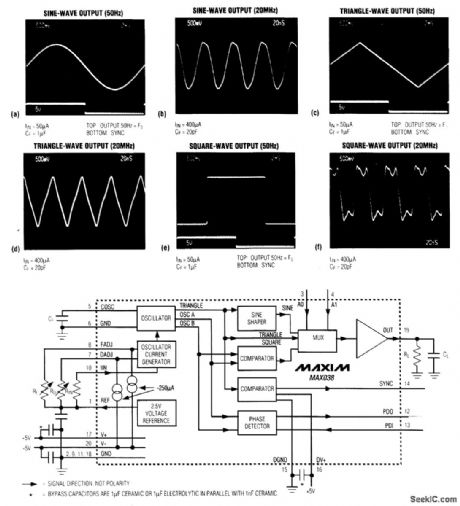


The MAX038 is a precision, high-frequency function generator that produces accurate sine, square, triangle, sawtooth, and pulse waveforms with a minimum of external components. The internal 2.5-V reference (plus an external capacitor and potentiometer) lets you vary the signal frequency from 0.1 Hz to 20 MHz. An applied ± 2.3-V control signal varies the duty cycle between 10 and 90 percent, enabling the generation of sawtooth waveforms and pulse-width modulation. A second frequency-control input-used primarily as a VCO input in phase-locked-loop applications-provides ± 70 percent of fine control. This capability also enables the generation of frequency sweeps and frequency modulation. The frequency and duty-cycle controls have minimal interaction with each other. All output amplitudes are 2 VP-P, symmetrical about ground. The low-impedance output terminal delivers as much as ± 20 mA, and a two-bit code applied to the TTL-compatible A0 and Al inputs selects the sine, square, or triangle output waveform: A0 A1 WAVEFORM X 1 sine wave 0 0 Square wave 1 0 Triangle waveX=Don’t Care (View)
View full Circuit Diagram | Comments | Reading(2119)
_LED_ROCKET_COUNTDOWN_LAUNCHER
Published:2009/7/13 21:53:00 Author:May

A 4011 quad two-input NAND gale and a 4017 decade-counter/divider IC are the heart of the launcher Transistor Q1,an IRF520 hexFET,sends the current through the igniter fuse to fire the rocket engine Two gates of a 4011 NAND gate,IC2-b and IC2-c,are connected in a low-frequencyoscillator circuit,with R5 and C3 setting the oscillator's frequency.Another gate of that IC,IC2-a,starts the countdown and sets pin 15 of the 4017 to the Run condition The IC's fourth gate,IC2-d,inverts and buffers the oscillator's output and supplies the clock input to pin 14 of the 4017. The 10 LEDs indicate the count. When the last one (LEDl) turns on, pin 11 goes high, turning Q1 on and firing the igniter fuse. The last LED, LED1, will remain on until S1 is switched off. The countdown can be halted by closing S3. Opening S3 continues the countdown. (View)
View full Circuit Diagram | Comments | Reading(1355)
LIMITING_PREAMP_FOR_FM
Published:2009/7/13 21:52:00 Author:May


All four sections of Motorola MC3401 quad amplifier are used as intelface between high-impedance microphoneand FM modulator to provide preemρhasis response of 6 dB per octave between 300 and 3000 Hz, with 6-dB per octave rolloff beyond. lncludes amplitude limiter to prevent peak deviation of transmitter from exceeding allowed maximum. U1D forms active fillter acting with passive filter following limiter to give low-pass filter having attenuation of at least 12 dB per octave above 3 kHz.-D. Aldridge, An Economical FM Transmitter Voice Processor from a Single IC, Motorola, Phoenix, AZ, 1975. EB-57.
(View)
View full Circuit Diagram | Comments | Reading(708)
14_MHz_VFO_USING_DOUBLER
Published:2009/7/13 21:50:00 Author:May

Developed for use with 20-meter low-power (QRP) transceiver. Push-push doubler avoids instability problems of 14-MHz oscillator and minimizes chirp during CW transmit periods. Uses lowdrift series-tuned Colpitts oscillator operating at 7 MHz, with source-follower buffer separating it from doubler. Adjust dynamic balance -control R1 of doubler for best output waveform purity. Capacitors marked P are polystyrene, and SM are silver mica, Article stresses importance of choosing and using components that minimize drift.-D. DeMaw, VFO Design Techniques for Improved Stability, Ham Radio, June 1976, p 10-17.
(View)
View full Circuit Diagram | Comments | Reading(1929)
SINGLE_IC_BATTERY_BACUP_MANAGER
Published:2009/7/13 21:49:00 Author:May

Instruments powered by a wall adapter with battery backup typically diode-OR the battery and wall-adapter connections. That arrangement carries a penalty, however-the diode in series with the battery limits the minimum voltage at which the battery can supply power. One alternative is a dual-comparator/reference IC, which monitors the battery and wall-adapter voltages with respect to its internal reference voltage. The open-drain output of comparator B (with pull-up to 3.3 V) provides a low-battery warning in the form of a low-to-high transition when battery voltage drops to 3.6 V. The open-drain output of comparator A (with pull-up to 9 V) flags low wall-cube voltage in the same way, with a warning threshold of 3.9 V. Comparator A also controls the PMOS switch Q1, which replaces the OR-connection diode in a conventional circuit. When wall power is removed, Q1 turns on and provides a low-resistance path from battery to regulator. (View)
View full Circuit Diagram | Comments | Reading(749)
5_MHz_±_500_kHz
Published:2009/7/13 21:49:00 Author:May
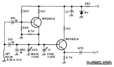
Developed for use as separate VFO control for transmitting and receiving frequencies in amateur transceiver. Capacitors marked M should be mica. Fine-tuning control covers ±20 kHz range. Will operate almost anywhere in HF range with appropriate change in coil. Output is 4 V P-P.-An Accessory VFO-the Easy Way, 73 Magazine, Aug. 1975, p 103 and 106-108. (View)
View full Circuit Diagram | Comments | Reading(1279)
FULL_WAVE_POWER_CONTROL
Published:2009/7/13 21:46:00 Author:May

Bidirectional three-layer trigger for triac allows triggering on both half-cycles at point determined by setting of 1-megohm pot. Triac rating determines size of load that can be handled.- SCR Power Control Fundamentals, Motorola, Phoenix, AZ, 1971, AN-240, p 6.
(View)
View full Circuit Diagram | Comments | Reading(654)
600_W_HALF_WAVE
Published:2009/7/13 21:45:00 Author:May

UJT serves as trigger for thyristor in circuit that provides power control for load only on positive half-cycles. Thyristor acts also as rectifier, providing variable power determined by setting of RT during positive half-cycle and no power to load during negative halfcycle.-D. A. Zinder, Unijunction Trigger Circuits for Gated Thyristors, Motorola, Phoenix, AZ, 1974, AN-413, p 3.
(View)
View full Circuit Diagram | Comments | Reading(3070)
BIQUINARY_DECADE_WITH_NIXIE_INDICATORS
Published:2009/7/13 21:44:00 Author:May
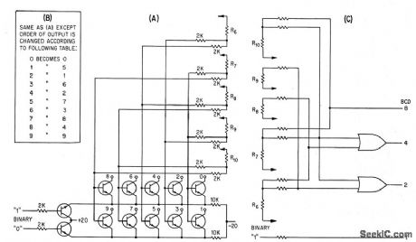
Transistor terminals 0 to 9 represent connections to Nixie indicator. Which requires no buffers. Counting rate can exceed 500 Mc, using 2N2708 transistors. Bi-quinary decade connections, shown at right and in table, permit easy conversion to bcd. –R. Engelmann. B-Quinary Scaling: Accuracy and Simplicity at 500 Mc. Electronics.36:46,p34-36. (View)
View full Circuit Diagram | Comments | Reading(823)
AUTO_SECURITY_DEVICE_1
Published:2009/7/13 21:44:00 Author:May

Combining two functions in one, this circuit is both a passive cutoff device and a fake car alarm Depressing S1 with the key in the RUN position disables the flasher and allows the car to start. (View)
View full Circuit Diagram | Comments | Reading(667)
18_2_MHz_FRONT_END
Published:2009/7/16 3:15:00 Author:Jessie
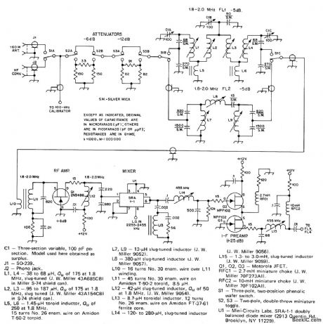
Includes enough attenuation for comfortable listening even when nearby high-power amateur station comes on air. Used with downconverter to cover 80 meters through 10 meters. Fixed-tuned 1.8-2 MHz bandpass filter FL2 eliminates need for repeaking three-pole tracking filter FL1 when tuning in band. RF amplifier Q1 compensates for filter loss by giving maximum of 6-dB gain. Double-balanced diode-ring mixer U1 handles high signal levels and has good port-to-port signal isolation. High-pass diplexer network at output of IC mixer U1 improve noise performance without degrading 455-kHz IF. Output goes to IF filter. Two-part article all other circuits of receiver. -D. DeMaw, His Eminence-the Receiver, QST, Part 1- June 1976, p27-30 (Part 2-July 1976, p 14-17).
(View)
View full Circuit Diagram | Comments | Reading(1185)
HIGH_PRECISION_AUTO_TACHOMETER
Published:2009/7/16 3:15:00 Author:Jessie
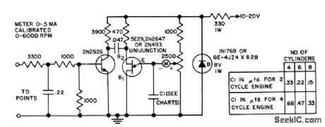
For auto ignition system having 12-v negative ground. Gives ultralinear readings on meter scale. Transistor Manual, Seventh Edition, General Electric Co., 1964, p 380. (View)
View full Circuit Diagram | Comments | Reading(617)
TRANSFLUXOR_OSCILLATOR
Published:2009/7/16 3:15:00 Author:Jessie

Holds frequency setting for many hours after removal of control signal. Operates between 100 kc and 1 Mc. Gives square-wave output.-R. J. Sheirn, Transfluxor Oscillator Gives Drift-Free Output, Electronics, 33:10, p 48-49. (View)
View full Circuit Diagram | Comments | Reading(1287)
4224_MHz_POWER_AMPLIFIER
Published:2009/7/13 21:44:00 Author:May

Used in local oscillator chain of 1296-MHz SSB transceiver to boost 10-mW output of chain to 500 mW as required for driving final diode-type tripler stage. Sections are connected together with miniature 50-ohm coax.-H. P. Shuch, Easy-to-Build SSB Transceiver for 1296 MHz, Ham Radio, Sept. 1974, p 8-23.
(View)
View full Circuit Diagram | Comments | Reading(746)
MONOCHROMATOR_PREAMP
Published:2009/7/16 3:13:00 Author:Jessie
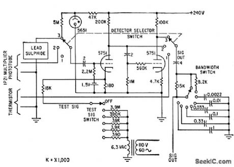
Used in scanning missile plumes to identify missile. Input may be either multiplier phototube or lead sulfide detector covering range from 0.35 micron in visible spectrum to 2.9 microns in infrared. Bias for lead sulfide detector is provided by 5651 regulator across plate supply. Test voltage is fed to cathode of first stage for gain calibration.-J. N. Day, Jr., Spectrometric Analysis of Missile Flights, Electronics, 33:21, p 86-88. (View)
View full Circuit Diagram | Comments | Reading(652)
LINE_POWERED_SWITCH
Published:2009/7/13 21:43:00 Author:May

When AC line twitch is closed, power is not applied to load until after line voltage next goes through zero. Identical circuits control each half of AC cycle. Transistor turn-on at 1.4 V prevents SCR from triggering until 0.013 ms (less than one-third electrical degree) after next zero-crossing point.-A. S. Roberts and O. W. Craig, Efficient and Simple Zero-Crossing Switch, EDN|EEE Magazine, Aug. 15, 1971, p 46-47. (View)
View full Circuit Diagram | Comments | Reading(665)
NINE_BIT_WORD_GENERATOR
Published:2009/7/16 3:13:00 Author:Jessie
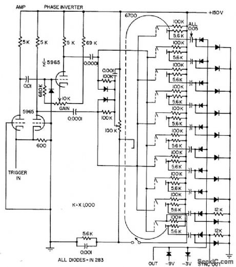
Beam-switching tube provides arbitrary nine-bit words at pulse rates from few cps to 1 Mc, for testing digital systems. Output can be changed from spike to square wave by changing plug-in capacitors.-R. R. Hartel, Word Generator for Digital Testing, Electronics, 31:9, p 71. (View)
View full Circuit Diagram | Comments | Reading(682)
MAGNETIC_TAPE_CONTROL_OF_ENGINE
Published:2009/7/16 3:13:00 Author:Jessie

Auto engine parameters are recorded during road tests, and tapes are then used to program laboratory engine to simulate further tests. Synchronous switches Q2-Q3 and Q4-Q5, driven by line-frequency square-wave generator, operate as line-synchronous spdt switch, to place tape signal and lab-engine feedback signal on line alternately and synchronously with line voltage. Frequency-measuring circuit develops d-c voltage proportioned to input frequency. Output is used to drive two-phase motor that controls lab engine parameter.-V. C. Vanderbilt and C. L. Zimmer, Magnetic Tape Recorder Programs Engine Dynamometer Tests, Electronics, 33:51, p 74-77. (View)
View full Circuit Diagram | Comments | Reading(538)
ROCKET_LAUNCHER_IGNITER_CIRCUIT
Published:2009/7/13 21:43:00 Author:May

An ISD1000A chip (IC1) containing a previously recorded message is connected in a simple playback-only circuit that operates when power is supplied by closing the START switch (S1). A 7805 voltage regulator, IC3, is used to drop the 12-V input voltage to 5 V. When the audio message is completed, IC1 produces a 16-ms low output pulse at pin 25. That low output pulse is fed to the input, pin 5, of a monostable multivibrator, IC2. That IC produces a long timed output pulse at pin 6, which turns Q1 on, supplying power to the igniter and firing the rocket engine. This circuit contains several safety features. Switch S2 removes power from the igniter fuse. One gate of a 4011 quad twoinput NAND gate (IC4-a) keeps the 4528B monostable multivibrator from misfiring and igniting the rocket motor prematurely. When the Start switch is first activated, IC4-a's input goes high while C4 is charging up, and its output at pin 3 goes low, keeping IC2 from responding to any false input pulse at pin 5. IC4-a's pin 3 clamps the input of Q1 to ground, through Dl, keeping it turned off. After a few seconds, C4 is fully charged and IC4-a's output goes positive, enabling IC2 and allowing Q1 to operate. Though not shown in the figure, the inputs of the quad IC's three unused gates (IC4-b to IC4-d, pins 5, 6, 8, 9, 12, and 13) must be tied to ground. (View)
View full Circuit Diagram | Comments | Reading(1408)
| Pages:677/2234 At 20661662663664665666667668669670671672673674675676677678679680Under 20 |
Circuit Categories
power supply circuit
Amplifier Circuit
Basic Circuit
LED and Light Circuit
Sensor Circuit
Signal Processing
Electrical Equipment Circuit
Control Circuit
Remote Control Circuit
A/D-D/A Converter Circuit
Audio Circuit
Measuring and Test Circuit
Communication Circuit
Computer-Related Circuit
555 Circuit
Automotive Circuit
Repairing Circuit