
Circuit Diagram
Index 664
UPWARD_SCALING
Published:2009/7/15 22:23:00 Author:Jessie

Output of AD580 threeterminal voltage regulator is multiplied in shunt regulator loop using opamp A,. Resulting reference voltage VEEF is scaled upward by reciprocal of feedback divider R1/R2. Resulting reference is immune to input variations. Reference output range is from 5 V up to voltage limit of opamp used. If desired, reference value can be programmed via R1. LED lights to show proper operation of circuit.-W. G. Jung, Programmable Voltage Reference is Stable, yet Simple, EDN Magazine, Nov. 5, 1975, p 98 and 100. (View)
View full Circuit Diagram | Comments | Reading(906)
DUAL_FUNCTION_SWITCH
Published:2009/7/14 1:05:00 Author:May

Pressing switch for less than 3 s produces single output pulse about 5μs wide. When switch is pressed longer than 3 s, single pulse is generated as before, and scan oscillator is turned on 3 s later. Oscillator runs as long as switch is held down, for producing repetitive stepping motion. Applications include positioning of test probes on single semiconductor chip or on wafer of several hundred chips, or indexing device either step by step or automatically through desired number of steps.-J. McDowell, Single Switch Controls Two Functions, EDN Magazine, April 5, 1974, p 78 and 80. (View)
View full Circuit Diagram | Comments | Reading(717)
MAGIC_WAND
Published:2009/7/15 22:22:00 Author:Jessie


This device is easy to use: Just aim the wand at a light source and listen to the tone. Two gates, IC1-a and IC1-b, of a quad two-input NAND gate are connected in an audio-oscillator circuit with R1, the photocell (R2), C1, and C2setting the tone of BZ1. When the photocell is aimed at alight source, its resistance drops and the oscillator's output tone increases in frequency. When either of tone switches (S1 or S2) is presse, the frequency range goes up. Pressing S2 shifts the oscillator into its highest-frequency range. Only one tone switch can be pressed at a time; if both switches are pressed simultaneously, the output stops. (View)
View full Circuit Diagram | Comments | Reading(859)
+82_V
Published:2009/7/15 22:22:00 Author:Jessie

Regulation is 0.01 mV/V for inputs of 10.3-22 V, and temperature stability is ±0.05% from -55℃ to 125℃. Short-circuit protection for reference is provided intemally. Uses National LM101, LM301A, or equivalent opamp.-D. W. Nelson, Introduction to Operational Amplifiers, Ham Radio, March 1978, p 48-60. (View)
View full Circuit Diagram | Comments | Reading(813)
PUT_CONTROLS_SCR
Published:2009/7/14 1:05:00 Author:May

Programmable unijunction transistor Q2 provides phase control for both halves of AC line voltage by triggering SCR connected across bridge. Relaxation oscillator formed by Q2 varies conduction interval of Q1 from 1 to 7.8 ms or from 21.6° to 168.5°, to give control over 97% of power available to load.-R. J. Haver and B. C. Shiner, Theory, Characteristics and Applications of the Programmable Unijunction Transistor, Motorola, Phoenix, AZ, 1974, AN-527, p 10. (View)
View full Circuit Diagram | Comments | Reading(1597)
WIDE_INPUT_VOLTAGE_RANGE
Published:2009/7/15 22:21:00 Author:Jessie

Power for LM199 temperature-stabilized voltage reference is obtained from output of LM108A buffer opamp, to permit use with to -25 V supply. 80K resistor is used in unregulated input to make circuit start properiy when power is applied.- Linear Applications, Vol. 2, National Semiconductor, Santa Clara, CA, 1976, AN-161, p 6. (View)
View full Circuit Diagram | Comments | Reading(922)
FET_DPDT
Published:2009/7/14 1:05:00 Author:May

Uses FETs as switching elements for transferring VFO and carrier oscillator signals between first and second mixers of SSB transceiver. Transmitter key line is at +13 V on receive and 0 V on transmit, and T line has opposite voltages. On receive, Q304 and Q305 are pinched off by about +10 V, while Q303 and Q306 are conducting with only about +0.7 V on their gates. VFO signal then flows to first mixer and carrier oscillator to second mixer. On transmit, conditions are opposite.-J. Schultz, CQ Re-views: The Atlas 210 and 215 SSB Transceivers, CQ, May 1975, p 22-27 and 65. (View)
View full Circuit Diagram | Comments | Reading(673)
SIGNAL_CONTROLLED_SWITCH
Published:2009/7/14 1:04:00 Author:May

This signal-controlled switch actuates or deactuates AF equipment, including preamplifiers, power amplifiers, and filters. It is particularly useful for battery-operated equipment because, owing to the low current drain of 12 to 14μA, there is no need to switch the AF equipment off. When the switch has not detected any AF signal for 10 seconds, it switches off the supply to the equipment. (View)
View full Circuit Diagram | Comments | Reading(1062)
NEGATIVE_SPDT
Published:2009/7/14 1:03:00 Author:May

Developed for driving R/2R ladder network in D/A conveners. Signal input or reference voltage range is 0 to -12 V. With logic 0, R1 forward-biases Q2 and O3; Q2 then switches output to ground, and Q3 clamps base of Q1 to ground to keep it off. With logic 1, D1 and D2 conduct and make Q1 switch on.-J, Cohen, Solid-State Signal Switching: It's Get-ting Better All the Time, EDN Magazine, Nov. 15, 1972, p 22-28. (View)
View full Circuit Diagram | Comments | Reading(628)
FULL_RANGE_CONTROL
Published:2009/7/14 1:02:00 Author:May

Triggered triac is used with double phase-shift network to obtain reliable triggering at conduction angles as low as 5°, as required for control of incandescent lamps and some motors. Triac rating determines size of load.- SCR Power Control Fundamentals, Motorola, Phoenix, AZ, 1971, AN-240, p 6. (View)
View full Circuit Diagram | Comments | Reading(1043)
SYNCHRONIZED_SWITCHING
Published:2009/7/14 1:02:00 Author:May

Transients occurring during switching between two amplifier channels are attenuated by synchronizing turn on of one switch in DG181 JFET analog switch with turnoff of other switch. Switching action is controlled by logic input,- Analog Switches and Their Applications, Siliconix, Santa Clara, CA, 1976, p 7-61. (View)
View full Circuit Diagram | Comments | Reading(694)
CAPACITOR_COUPLED_DRIVE_FOR_SWITCHING_TRANSISTOR
Published:2009/7/14 1:02:00 Author:May
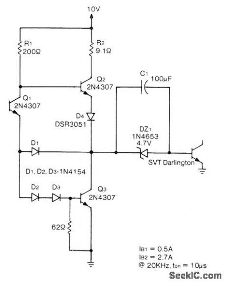
TRW SVT6062 power Darling-ton switching transistor is used in grounded-emitter connection in which negative bias required for turnoff is created by charging C1 during ON interval. Zener limits charge on C1 and provides path for base drive current to Darlington. Diodes give faster response to input signal by preventing Q3 from saturating. Grounding base of Q1 makes Darlington con duct, whereas high input level to Q1 initiates turnoff. Circuit will operate at pulse widths down to 5μs.-D. Roark, Base Drive Considerations in High Power Switching Transistors, TRW Power Semiconductors, Lawndale, CA, 1975, Application Note No. 120, p 7. (View)
View full Circuit Diagram | Comments | Reading(966)
NONVOLATILE_LATCH
Published:2009/7/14 1:00:00 Author:May

Design shown for latch gives immunity to interfering noise pulses on command line and prevents loss of essential data bit during unexpected power-line interruption. Subminiature saturable transformers in positive feedback paths between two gates of latch prevent instantaneous change of state. Transformers remain magnetically biased in positive or negative saturation even without circuit power, to provide pretransient-state reference to which latch must return when power is reapplied.-G. E. Bloom, Add Nonvolatility to Your Next Latch Design, EDN Magazine, Jan. 5, 1978, p 80 and 82. (View)
View full Circuit Diagram | Comments | Reading(869)
SOUND_ACTIVATED_CHRISTMAS_TREE
Published:2009/7/14 1:00:00 Author:May

Switch S1,an ON/OFF switch,directs power from the 9-V battery to the circuit The first half of an LM358,U1A,is configured as a high-gain amplifier Resistors R3 and R4 form a voltage divider that sets the bias voltage at put 3,holding the amplifier in the Off state Resistors R1 and R2,also forming a voltage divider,set the bias point for the microphone When the audio input signal produced by the microphone exceeds the bias voltage,U1A turns on and operates as a high-gain amplifier(with the gain being set by resistor R5) Capacitor C1 couples the microphone’s signal to the amplifier’s inverting input,put 2 Resistor R6 and capacitor C2 are used as a filter network for the Op amp The second half of U1,U1B,is configured as a peak signal detector it is triggered by the negative half-cycle output of U1A Each negative half-cycle of the signal produces a positive clock signal to the input of U2,the seven-stage binary ripple counter Capacitor C3 Stores the average peak level of the input signal,and resistor R7 determines C3’s discharge tune.Integrated circuit U2 produces a binary count on its Q3 through Q6 outputs that is proportional to the frequency of the audio input signal The output of Q3 is connected,via capacitor C4,to the ENABLE pm of U3 When the input audio signal causes U2 to conduct,the relatively high-frequency output of Q3 enables U3 Resistor R3 maintains U3 In the Disabled mode Ill the absence of any audio input signal U3’s output lines,X0 through X7,are turned on and off in rapid Sequence,causing the LEDs to display a random flashing effect that is proportional to the original、al audio signal (View)
View full Circuit Diagram | Comments | Reading(1288)
LOGIC_CONTROLLED_ANALOG_SWITCH
Published:2009/7/14 1:00:00 Author:May

2N4860 JFETs were chosen for low leakage and 25-ohm ON resistance in switching circuit. LM102 opamp serves as voltage buffer. DS7800 IC provides switch drive under control of DTL or TTL levels.- FET Databook, National Semiconductor, Santa Clara, CA, 1977, p 6-26-6-36. (View)
View full Circuit Diagram | Comments | Reading(772)
SWITCHING__SINGLE_SUPPLY_OPAMPS
Published:2009/7/14 0:58:00 Author:May

DG301 low-power analog switch serves as interface between TTL control input and DC-coupled opamp pair Logic level determines which opamp is connected to single output.- Analog Switches and Their Applications, Siliconix, Santa Clara, CA, 1976, p 7-88-7-89. (View)
View full Circuit Diagram | Comments | Reading(747)
ACTIVE_LOW_TRIAC_INTERFACE
Published:2009/7/14 0:58:00 Author:May

With connection shown for interface transistor Q1,typical CMOS gate triggers triac when gate output goes low, for switching of 25-W lamp load,-A. Pshaenich, Interface Techniquos Between Industrial Logic and Power Devices,″Motorola, Phoenix,AZ,1975,AN-712A,p12. (View)
View full Circuit Diagram | Comments | Reading(697)
AC_SPDT
Published:2009/7/14 0:56:00 Author:May

Complementary NPN and PNP transistors provide single-pole double-throw switching action for AC signals, as required in some digital-to-analog converter applications. Circuit switches between ground and signals of up to±5 V. Output transistor pair will toggle with unipolar drive.-J. Cohen, Solid-State Signal Switching : It's Getting Better All the Time, EDN Magazine, Nov. 15, 1972, p 22-28. (View)
View full Circuit Diagram | Comments | Reading(2132)
CABLE_TESTER_TRANSMITTER
Published:2009/7/15 23:28:00 Author:Jessie
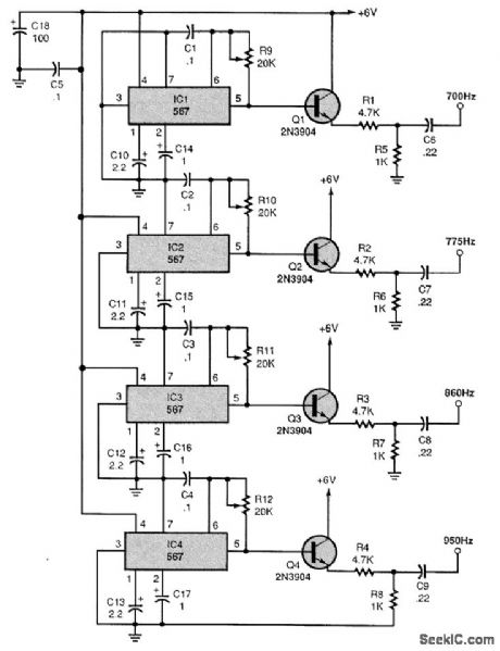
Four 567 tone-decoder ICs, IC1 to IC4, are used to generate four different audio frequencies between 700 and 950 Hz. The capacitor from pin 6 of each 567 to circuit ground, along with the resistor between pins 5 and 6, sets the operating frequency. A 2N3904 NPN transmitter is connected in an emitter-follower circuit to isolate the ICs from output loading. Each output supplies a different audio tone to four wires in a cable. (View)
View full Circuit Diagram | Comments | Reading(2451)
50_dB_ATTENUATION_CONTROL
Published:2009/7/15 23:27:00 Author:Jessie
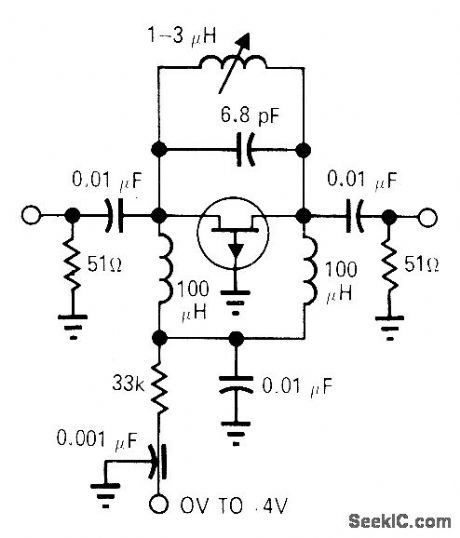
Low-cost FET in pi network serves as resistive attenuator providing up to 50-dB attenuation of 30-MHz level-controlled signal source by varying DC control voltage over range of 0 to 4 V. Tank circuit across source-drain leads of FET keeps phase shift under 2° over entire attenuation range. FET type is not critical -E. E. Baldwin, Voltage-Controlled Attenuator Has Minimum Phase Shift, EDN|EEE Magazine, Nov. 15, 1971, p 40. (View)
View full Circuit Diagram | Comments | Reading(773)
| Pages:664/2234 At 20661662663664665666667668669670671672673674675676677678679680Under 20 |
Circuit Categories
power supply circuit
Amplifier Circuit
Basic Circuit
LED and Light Circuit
Sensor Circuit
Signal Processing
Electrical Equipment Circuit
Control Circuit
Remote Control Circuit
A/D-D/A Converter Circuit
Audio Circuit
Measuring and Test Circuit
Communication Circuit
Computer-Related Circuit
555 Circuit
Automotive Circuit
Repairing Circuit