
Circuit Diagram
Index 659
STEPPER_MOTOR_SPEED_AND_DIRECTION_CONTROLLER
Published:2009/7/15 23:24:00 Author:Jessie

This new circuit uses four chips, with an option of using just three (the flip-flops and AND gates can be combined). The rate of clock pulses determines the motor's rpm. Switching transistors can replace the relays to increase the circuit's efficiency. This circuit drives a stepper motor whose speed depends on clock rate. Standard SS1 LSTTL chips are used. Switching transistors can be used in place of the solid-state relays to improve the circuit's efficiency. This new circuit uses four chips, with an option of using just three (the flip-flops and AND gates can be combined). The rate of clock pulses determines the motor's rpm. Switching transistors can replace the relays to increase the circuit's efficiency. This circuit drives a stepper motor whose speed depends on clock rate. Standard SS1 LSTTL chips are used. Switching transistors can be used in place of the solid-state relays to improve the circuit's efficiency. (View)
View full Circuit Diagram | Comments | Reading(1488)
DUTY_CYCLE_LIMITER
Published:2009/7/15 23:23:00 Author:Jessie

When duty cycle exceds 1%, countdown begins and duty cycle is held at about 1%. Uses voltage-controlled useable mvbr consisting of Q2, Q3, and Q4, which runs unsynchronized with input prf.-C. Samocki, Duty-Cycle Limiter, EEE, 13:9, p 76. (View)
View full Circuit Diagram | Comments | Reading(950)
HAMMER_DRIVER_FOR_COMPUTER_LINE_PRINTER
Published:2009/7/15 23:23:00 Author:Jessie

Gale turnoff scr overdrives load solenoid momentarily by connecting it across 350-v bus and disconnecting before over heating occurs. Load current rise and fall limes are less than one millisec.-D. R. Grafham, Now the Gale Turnoff Switch Speeds Up D-C Switching, Electronics, 37:12, p 64-71. (View)
View full Circuit Diagram | Comments | Reading(687)
ACTIVE_LOAD_RESISTOR
Published:2009/7/15 23:22:00 Author:Jessie


The design idea presented here concerns an active power resistor. It can be used as a load resis-tor when probing or servicing power supplies. The circuit can work in three different modes. It can act as a constant resistor (mode CR), or as a constant current from a supply of any positive voltage. Finally, it can be in constant-voltage mode (CV), in which the circuit loads the voltage across supply terminals to a constant value adjusted by the user. The power MOSFET transistor Q1 works as a resistive component. The transistor gate is controlled by an op amp (U1B). The feedback voltage, which can be selected by switch SW2, is connected to the amplifier's inverting input. In CC and CR modes, the feedback voltage is the voltage between the source resistor (R1) terminals, which is proportional to the amplifier supply voltage (VB) through a voltage-divider circuit (R4-R5). The amplifier noninverting input is controlled by a control voltage. The control-voltage input can be selected by switch SW1. In CR and CV modes, that input is the resistor input voltage (Vin), and in CC mode, it is the amplifier supply voltage (VB). The control voltage is set in voltage divider R2-R3 to a proper value to control the amplifier. The other op amp (U1A) protects the MOSFET transistor. It is con-trolled by a resistor bridge circuit consisting of three resistors (R7 through R9) and an NTC resistor. The NTC is in contact with the transistor cooling element. With moderate element temperatures, the output voltage of U1A is high, and thus has no effect on the transistor gate because of the reverse-biased diode (D1). If the element temperature becomes high, the amplifier output has a zero value, which takes the transistor gate voltage to zero through the diode. The amplifiers also can be powered directly from the resistor input voltage. This circuit can work in CR mode without any control voltage. In CC and CV modes, however, it should be controlled by the external voltage CC/CV input. The circuit acts in CR mode as a resistor that has a resistance of
The required resistance value can be adjusted by potentiometer R3. In CC mode, the circuit sinks a current The sink current
also can be adjusted by potentiometer R3 In CV mode,the voltane between theLerminals of the resistor is:
The required constant voltage can be adjusted by both R3 and R5 (View)
View full Circuit Diagram | Comments | Reading(5251)
SYMMETRICAL_LIMITER
Published:2009/7/15 23:22:00 Author:Jessie

Used in visual receiver of microwave relay. Signal is fed through triode cathode follower and diode-coupled to grid of pentode. D1 cuts off on positive r-f swing above d-c bias set by R1 and R2, to prevent grid of V5B from going positive and provide clipping on negative swing.-T. G. Custin and J. Smith, Relay System Diplexes Audio and Color Video, Electronics, 31 :25, p 64-67. (View)
View full Circuit Diagram | Comments | Reading(609)
COAXIAL_CABLE_DRIVER
Published:2009/7/15 23:21:00 Author:Jessie
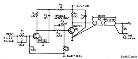
Can drive digital information through long lengths of coaxial cable. Will send pulses with 30-nsec rise and fall time through 1,155 feet of 50-ohm RG/ 188U or through 650 feet of 93-ohm RG/ 62U.-B. Strunk, Coaxial Cable Driver Circuit, EEE, 13:5, p 43-44. (View)
View full Circuit Diagram | Comments | Reading(1895)
RADAR_NOISE_CLIPPER_LIMITER
Published:2009/7/15 23:21:00 Author:Jessie

Used in plotting amplitude-distribution density of noise and vibration signals over range of 1 to 10,000 cps. Section A samples d-c biased input signal between zero and positive half of slice width. Section B similarly handles negative half. Output of B is inverted and biased in d-c amplifier to produce positive square wave. Recorder plots average of combined outputs from A and B sections.-D. J. Zoll, Simple Plotter Analyzes Radar Noise Rapidly, Electronics, 31:11, p 162-164. (View)
View full Circuit Diagram | Comments | Reading(644)
GEIGER_MUELLER_TUBE_CIRCUIT
Published:2009/7/14 2:21:00 Author:May

A GM tube is useful for detecting radioactivity. The tube is constructed with a cylindrical electrode (cathode) surrounding a center electrode (anode). The tube is evacuated and filled with a neon and halogen gas mixture. A voltage potential of 500 V is applied across the tube, through a 10-MΩ current-limiting resistor (R1). The detection of radiation relies upon its ability to ionize the gas in the GM tube. The tube has an extremely high resistance when it is not in the process of detecting radioactivity. When an atom of the gas is ionized by the passage of radiation, the free electron and positive ionized atom that are created move rapidly toward the two electrodes in the GM tube. In doing so, they collide with and ionize other gas atoms, which creates a small avalanche effect. This ionization drops the resistance of the tube, allowing a sudden surge of electric current that creates a voltage across the resistor R2, which can be seen as a pulse. (View)
View full Circuit Diagram | Comments | Reading(2640)
DUAL_BATTERU_CAPACITY_INDICATOR
Published:2009/7/14 2:19:00 Author:May

This indicator circuit uses two separate expanded meter scale circuits and can be calibrated for use with two different types of batteries. (View)
View full Circuit Diagram | Comments | Reading(873)
2_METER_FM_EXCITER
Published:2009/7/14 2:19:00 Author:May

Includes both deviation and microphone gain controls. Low-pass filter following limiter eliminates raspy voice signal. Input takes either carbon or transistor-amplified dynamic microphones. Phase modulation used is suitable for multichannel operation and frequency synthesizers. Oscillator uses 12-MHz series-resonant crystals. Voltage regulator for oscillator, modulator, and audio stages minimizes effects of line-voltage variation and noise. Output power of 150-200 mW is enough to drive new TRW and Motorola RF power modules. Article gives construction and alignment details.-J. Vogt, High-Performance Two-Meter FM Exciter, Ham Radio, Aug. 1976, p 10-15. (View)
View full Circuit Diagram | Comments | Reading(1813)
5_W_ON_80_OR_40_m
Published:2009/7/14 2:17:00 Author:May

Single 6AQ5 operating from 200-V supply can cover all states and some DX with CE on 40 meters as low-power amateur radio station Antenna can be simple dipole 8 feet high L1 is 15 turns No 22 enamel on 11/4-inch plastic form, with 3 turns of insulated wire wound around cold end of L1 for L2 Article covers construction and operation and gives suitable 200-V voltage-doubling power supply circuit.-S.Dunn, ORP Fun on 40 and 80, 73 Magazine.Oct 1976, p 44-46. (View)
View full Circuit Diagram | Comments | Reading(858)
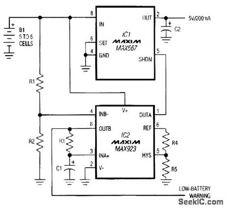
LOW_BATTERY_DETECTOR
Published:2009/7/14 2:17:00 Author:May
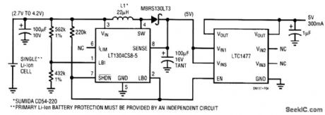
Low-voltage cutoff is desirable in battery-operated systems to prevent deep discharge damage to the battery. The LT1304 micropower boost regulator contains a low-battery detector which is active even when the regulator is shut down. The output of the detector controls both the LTC1477 and the LT1304 5-V boost regulator. In this application, the LTC1477 serves to protect against short circuits (850-mA limit selected) and completely disconnects the load under a low-battery condition. In shutdown, the circuit draws less than 25 μA from the battery. (View)
View full Circuit Diagram | Comments | Reading(0)
AC_POWER_CONTROLLER_FOR_VCR
Published:2009/7/14 2:15:00 Author:May
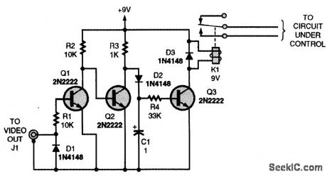
This circuit can be used to switch on a manual-control TV when a VCR signal is present. When the tape starts, video is present at J1 from the VCR video output jack. This is detected, and the dc produced in the detector (D1) circuit turns on Q1, cutting off Q2, and allowing relay driver Q3 to actuate the relay K1. (View)
View full Circuit Diagram | Comments | Reading(979)
ALARM_CONTROL
Published:2009/7/14 2:13:00 Author:May

Any input suitable for driving LED of optoisolator triggers triac for energizing load such as alarm gong. Transistors Q4 and Q5 of CA3096 array serve as comparator. Diode-connected transistor Q3, zener-connected transistor Q1, and 100-μF capacitor develop DC supply voltages from AC line.- Circuit ideas for RCA Linear ICs, RCA Solid State Division, Somerville, NJ, 1977, p 9. (View)
View full Circuit Diagram | Comments | Reading(830)
GEIGER_COUNTER_CIRCUIT
Published:2009/7/14 2:13:00 Author:May
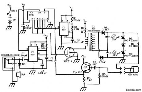
IC2 is a 555 timer set in astable mode. The signal from IC2 is presented to three gates on the 4049 IC1. The 4049 inverts the signal to give an optimum pulse width that switches Q1 on and off. The MOSFET(Q1),in turn,switches the current to a step-up transformer(T1). The stepped-up voltage from T1 first passes through a voltage doubler; the output voltage from this section is approxtmatety 600 to 700 V . Three zener diodes(D3,D4,and D5)are placed across the output of the voltage doubler to regulate the voltage to 500 V. This voltage is connected to the anode on the GM tube through a 10-MΩ resistor. When the GM tube detects a particle,a voltage pulse from the 100-kΩ resistor is amplified and clamped to VCC, Via Q2,an NPN Darlington transistor. The signal from Q2 is inverted by IC1,where it acts as a trigger signal to IC3. IC3 is another 555 timer. The output of IC3 Via pin 3 flashes on LED and provides a click into either the speaker or the headphones . The circuit is powered by a 9-V alkaline battery and draws about 28 mA when not detecting. (View)
View full Circuit Diagram | Comments | Reading(2072)
PNP_SWITCHES
Published:2009/7/14 2:13:00 Author:May

This figure shows two examples of a transistor PNP switch∶ (a)a single transistor and (b)a Darlington transistor. (View)
View full Circuit Diagram | Comments | Reading(977)
LOW_BATTERY_MONITOR
Published:2009/7/14 2:12:00 Author:May
This circuit gives an early warning of declining battery voltage. Then, to allow a controlling processor time for emergency housekeeping chores, such as the storage of register data, the circuit delays system shutdown by a specified time interval (rather than waiting for battery voltage to decline further, to a specified lower level). Circuit components are chosen for low quiescent current, which protects discharged cells by minimizing the battery drain during shutdown: IC1 draws 1 μA, IC2 draws 3 μA, and R1 and R2 draw 3 μA, for a total shutdown current of about 7 μA. R1 and R3=1 MΩ, R2 =280 kΩ, R4=49.9 kΩ, R5=2.4 MΩ, and C1=3.9 μF
(View)
View full Circuit Diagram | Comments | Reading(1046)
SPDT_PIN_DIODE_HIGH_SOLATION_SWITCH_CIRCUIT
Published:2009/7/14 2:10:00 Author:May

This circuit is a basic SPDT PIN-diode switch using a series- and shunt-diode building block. Resistance R is chosen from Idiode =(Vcc-Vdiode)/R, where Idiode is the specified diode current and R is total dc circuit resistance. (View)
View full Circuit Diagram | Comments | Reading(704)
OPTOISOLATOR_AS_SOLID_STATERELAY
Published:2009/7/14 2:09:00 Author:May


Circult provides input protection of LED from overvoltage and reverse polarity,along with snubber network for handling inductive AC loads. Triac should be chosen to handle load.Safe input voltage range is 3-30 VDC.-P.O'Neil, Applications of the MOC3011 Traic Driver, Motorla,Phoenix,AZ,1978,AN-780,p 6. (View)
View full Circuit Diagram | Comments | Reading(1083)
NiCd_BATTERY_CYCLER
Published:2009/7/14 2:07:00 Author:May

The battery cycler works with NiCd configurations of between three and nine cells. Cell combinations are accommodated by selecting Z1, K1, and R3 based upon the number of cells in the battery pack. This circuit is basically composed of a voltage comparator (U1), a voltage reference (Z1), and a switch (Q1 and K1). The op amp (U1) compares the reference voltage generated by the zener diode (Z1) and the battery. When the battery voltage matches (or is less than) the reference, the switch is turned off and the battery is allowed to charge. While the battery voltage is above the reference voltage, it is discharged through resistor R3. The resistor has been selected to discharge the battery at a rate between 200 and 300 mA. This rate keeps the power dissipation in R3 below 3 W and reduces the risk of opening any fuses in the battery circuitry located in the portable equipment. The push-button switch (S1) initiates the discharge process. If the battery voltage is below the reference when S1 is pressed, the unit will not discharge the battery because the lower operating limit of the battery has already been exceeded. If your batteries are in this condition, charge them for 18 hours and measure the voltage. If the batteries are still below the cutoff voltage, the problem is with one or more cells in the battery pack. (View)
View full Circuit Diagram | Comments | Reading(1384)
| Pages:659/2234 At 20641642643644645646647648649650651652653654655656657658659660Under 20 |
Circuit Categories
power supply circuit
Amplifier Circuit
Basic Circuit
LED and Light Circuit
Sensor Circuit
Signal Processing
Electrical Equipment Circuit
Control Circuit
Remote Control Circuit
A/D-D/A Converter Circuit
Audio Circuit
Measuring and Test Circuit
Communication Circuit
Computer-Related Circuit
555 Circuit
Automotive Circuit
Repairing Circuit