
Circuit Diagram
Index 653
_10000_V
Published:2009/7/15 21:22:00 Author:Jessie

Uses LM301A opamp with 1N825 6.2-V zener reference diode (not zener regulator diode) to maintain stable DC voltage under severe combinations of temperature, shock, and vibration. Gain resistors R2 and R3 should have same 0.01%/℃ temperature coefficients as reference diode. R1 is RN55 511-ohm metal-film resistor, R2 is RN55E 6.04K metal-film resistor, and R3 is RN55E 3.57K metal-film resistor. R4 and R5 are gain trim resistors. R6 should equal parallel combination of R2 and R5. R8 is 10K cermet pot. with R7 (optional) 100K to 1 megohm. Article tells how to trim circuit for desired out-put and how to calculate values of resistors and temperature coefficients for other output volt-ages.-D. W. Ishmael, Precision +10.000 V DC Voltage Reference Standard, 73 Magazine, Sept. 1975, p 124-126. (View)
View full Circuit Diagram | Comments | Reading(1204)
NUMERICAL_DISPLAY
Published:2009/7/15 21:21:00 Author:Jessie

Either cold. cathode trigger tubes or transistors drive 10-digit cold-cathode indicator Tube.-M. A. Mac-Dougall, Using the Cold-Cathode Tube: Part 1, Electronics, 38:6, p 78-82. (View)
View full Circuit Diagram | Comments | Reading(1194)
34_V_RADIATION_HARD_ENED
Published:2009/7/15 21:20:00 Author:Jessie

Two-stage regulator is combined with special filter design that helps keep output voltage free of gamma-produced transients and RFI. Voltage divider using wirewound resistors provides 2-V output. Gamma radiation of 1,000,000 rads caused only 0.3% change in output voltages. Article covers procedure for designing and testing circuits that are to be operated in high-radiation environment.-A. J. Sofia, Designing a Radiation-Stable Voltage Reference, EDN Magazine, Sept. 15, 1970, p 39-41. (View)
View full Circuit Diagram | Comments | Reading(769)
_10__20_AND__30_V
Published:2009/7/15 21:34:00 Author:Jessie

Simple stacking arrangement of Precision Monolithics REF-01 voltage references gives near-perfect line regulation for inputs of 32 to 60 V, with output changes less than noise voltage of devices for input extremes. Any number of units can be stacked to obtain additional output voltages.- + 10 V Precision Voltage Reference, Precision Monolithics, Santa Clara, CA, 1977, REF-01, p 7. (View)
View full Circuit Diagram | Comments | Reading(775)
PREVENTS_AMPLIFIER_OVERLOAD
Published:2009/7/15 23:13:00 Author:Jessie
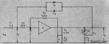
Zener 6.8-v diode shunts output while feedback diodes limit input. With input below 40 mv, output is below -5 v and diodes D1, D2, and D3 are biased off. When output exceeds -6.8 v, diodes act to damp output at -6.8 v und maintain linear voltage relationships within the amplifier, preventing its saturation and allowing recovery from overloads.-J. V. Dirocco and J. W, Peghiny, Low-Level Encoding Approach: Latest Details of Titan II Telemetery, Electronics, 35:47, p 36-39 (View)
View full Circuit Diagram | Comments | Reading(681)
BIDIRECTIONAL_ACTIVE_LOAD
Published:2009/7/15 23:13:00 Author:Jessie
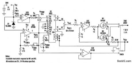
The design presented here is a single +9-V, battery-operated, bidirectional active load that can sink and source current. This is a low-power design, consuming only about 140μA. The power MOSFET selected (IRF530 N-channel and IRF9530 P-channel), after derating, accepts a maximum load of ±50V at ±5 A. The key to the design is having two different sets of voltage levels at Vx ,VY, and VSS1. One set is for current-sinking test, while the other is for current-sourcing test. (View)
View full Circuit Diagram | Comments | Reading(3424)
VIDEO_SIGNAL_PROCESSOR
Published:2009/7/15 23:12:00 Author:Jessie
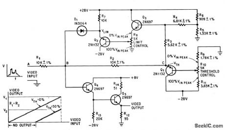
R10 adjusts threshold level and R8 adjusts limit level between which video input signal will be fed to crt display.-A. E. Popodi, Reliable Repertoire Of Display Circuits, Electronics, 38:2, p 60-66. (View)
View full Circuit Diagram | Comments | Reading(667)
CONSTANT_PULSE_WIDTH__ONE_SHOT
Published:2009/7/15 23:12:00 Author:Jessie
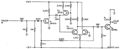
Monostable circuit holds pulse width constant within 0.5% from -65℃. Stages Q1 and Q2 form conventional one-shot. Use of differential amplifier for Q2 stabilizes base voltage for turn-on of Q2 near ground. Constant-current transistor Q3 minimizes effects of small voltage variations, and switching transistor Q4 provides 35-V output pulse with base line at ground.-R. Stevens, One-Shot Multi Produces Constant Pulse Width, Electronics, 34:13, p 74-75. (View)
View full Circuit Diagram | Comments | Reading(900)
MOBILE_DISCRIMINATOR_AND_LIMITER
Published:2009/7/15 23:11:00 Author:Jessie
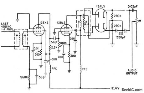
Two limiter stages in cascade precede Foster-Seely discriminator.-C. Gonzalez and R. J. Nelson, Design of Mobile Receivers with Low-Plate-Potential lubes, Electronics, 33:34, p 62-65. (View)
View full Circuit Diagram | Comments | Reading(661)
SCR_LATCHING_CIRCUIT_WITH_RATE_EFFECT_SUPPRESSION
Published:2009/7/15 23:09:00 Author:Jessie


With basic scr latching circuit (at left) for latching on lamp when input voltage level is exceeded, resetting of circuit by opening supply lead exposes scr to fast transients and possible turn-on due to rate effect. Adding 100,000-ohm resistor and using four-terminal silicon controlled switch suppresses rate effect.-R. A. Stasior, How to Suppress Rate Effect in PNPN Devices, Electronics, 37:2, p 30-33. (View)
View full Circuit Diagram | Comments | Reading(1199)
120_V_A_C_LATCH
Published:2009/7/15 23:06:00 Author:Jessie

Bidirectional controlled rectifier (G.E. Triac) replaces more complicated scr or power transistor circuits for static switching of a-c power circuits. Can be adapted to simulate action of magnetic starter for a-c motor Momentary closing of start switch (in circuit at right ) latches Triac on and starts motor-F. W. Gutzwiller, Simplified 120 VAC Latching Circuit, EEE, 13:8,p 77. (View)
View full Circuit Diagram | Comments | Reading(1763)
432_MHz_LOW_NOISE_PREAMP
Published:2009/7/15 23:04:00 Author:Jessie

Uses Fairchild FMT4575 transistor having 1.25-dB noise figure, equaling performance of best paramps at 432 MHz. Input matching circuit is low-loss low-Q L matching section L1-CR1. Value of blocking capacitor C1 is not critical, but should be low-loss high-Q type, Hot-carrier diode CR1 in matching section adds about 0.75 pF to circuit, and serves also as low-loss limiter that protects transistor from excessive RF. Zener-diode biasing permits direct grounding of emitter, is insensitive to transistor current gain, provides some DC protection to transistor, and requires no adjustments.-J. H. Reisert, Jr., Ultra Low-Noise UHF Preamplifier, Ham Radio, March 1975, p 8-19. (View)
View full Circuit Diagram | Comments | Reading(1143)
VOLTAGE_DIP_INDICATOR
Published:2009/7/15 23:03:00 Author:Jessie


Two neon lamps in parallel, with different striking voltages, form neon latch. After circuit is activated, next line voltage dip below preset level turns on lamp L. Circuit is then disabled until reset button is pressed.-T. D. Koranye, Thyratron Monitors Line-Voltage Dips, Electronics, 34;1, p126. (View)
View full Circuit Diagram | Comments | Reading(869)
SINGLE_IC_RADIO
Published:2009/7/15 23:02:00 Author:Jessie

National LM3909 IC is connected as detector-amplifier driving loud-speaker, with extremely low power gain giving continuous operation for 1 month from D cell. Tuning capability is comparable to that of simple crystal set. Provides acceptable volume from local station if used with efficient 6-inch 40-ohm loudspeaker. Coil is standard AM radio ferrite loopstick having tap 40% of turns from one end. Short antenna can be 10-20 feet, and long antenna can be 30-100 feet.- Linear Applications, Vol. 2, National Semiconductor, Santa Clara, CA, 1976, AN-154, p 8-9. (View)
View full Circuit Diagram | Comments | Reading(1360)
6_METER_PREAMP
Published:2009/7/15 23:01:00 Author:Jessie

Simple transistor circuit requires no tuning, draws less than 50mW from 9-V supply, and increases sensitivity of low-priced receiver without complicated impedance matching.-E. R. Davisson, Simple Six Pre-Amp, 73Magazine, Oct. 1974, p 111-112. (View)
View full Circuit Diagram | Comments | Reading(1131)
TRANSIENT_DETECTOR
Published:2009/7/15 23:00:00 Author:Jessie
Transient or other pulse at input turns on scr Q1, pulling in dpdt latching relay. Q2 then charges C through R2 until emitter voltage of Q2 is high enough to make it conduct and provide trigger pulse for Q3 to unlatch relay.-D. P. Lynch, Unijunction Transistor Tums off latching Relay, Electronics, 38:23, p 109. (View)
View full Circuit Diagram | Comments | Reading(1262)
RECEIVER_CHECKING_VFO
Published:2009/7/15 23:00:00 Author:Jessie
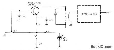
Simple variable-frequency oscillator is combined with attenuator network to generate signal of about 1 μV for checking performance of amateur radio receiver quickly. Attenuator is series arrangement of 47-, 100-, 100-, and 47-ohm resistors, with 1-ohm resistors going from each of the three junctions to ground. LC combinations are chosen for amateur band desired. Circuit will work down to at least 2 meters.-Is It the Band or My Receiver? , 73 Magazine, Oct. 1976, p 132-133.
(View)
View full Circuit Diagram | Comments | Reading(701)
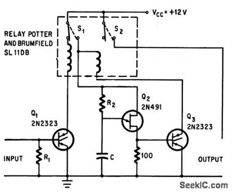
SCR_A_C_LATCHING_RELAY
Published:2009/7/15 22:59:00 Author:Jessie
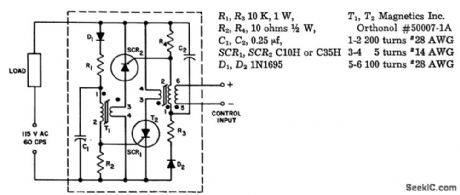
Relay is activated by d-c or a-c control current in single electrically isolated control winding. Can switch load power up to 1.7 kw. Uses magnetic firing circuit in which saturable core is not required to sustain gale voltage for full half-cycle, thereby permitting use of smaller core. Load current must be above 1 amp for conduction to be maintained.-Solid State Latching Relay, Electronic Circuit Design Handbook, Mactier Pub. Corp., N.Y., 1965, p 226. (View)
View full Circuit Diagram | Comments | Reading(934)
TRANSIENT_IMMUNE_SCR_LATCHING_CIRCUIT
Published:2009/7/15 22:58:00 Author:Jessie

With 100,000-ohm resistor of silicon controlled switch returned to +24 v, latching circuit for lamp is immune to transient spikes of up to 12 v as well as to rate effect when turned off.-R. A. Stasior, How to Suppress Rate Effect in PNPN Devices, Electronics, 37:2, p 30-33. (View)
View full Circuit Diagram | Comments | Reading(821)
POSITIVE_GATING_OF_CLOCK_PULSES
Published:2009/7/15 22:56:00 Author:Jessie
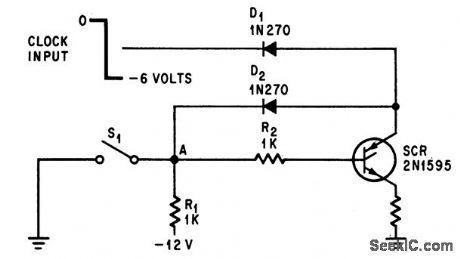
Adding scr latch to diode gate allows output to follow dock input when S1 is dosed. When S1 is open, output will be fixed at existing dock level, without putting extra count into register.-R. A. Wilson, Latching Gate Removes Counter Ambiguity, Electronics, 39:7, p 91-92. (View)
View full Circuit Diagram | Comments | Reading(567)
| Pages:653/2234 At 20641642643644645646647648649650651652653654655656657658659660Under 20 |
Circuit Categories
power supply circuit
Amplifier Circuit
Basic Circuit
LED and Light Circuit
Sensor Circuit
Signal Processing
Electrical Equipment Circuit
Control Circuit
Remote Control Circuit
A/D-D/A Converter Circuit
Audio Circuit
Measuring and Test Circuit
Communication Circuit
Computer-Related Circuit
555 Circuit
Automotive Circuit
Repairing Circuit