Signal Processing
RANDOM_NUMBER_GENERATOR
Published:2009/7/14 3:30:00 Author:May | From:SeekIC

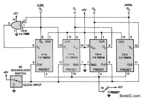
The 74574 flip-flops shown in the circuit are arranged to form a 4-bit shift register. Binary data enter the D0 input on U1-a and are sequentially shifted to each output (Q0, Q1, Q2, Q3) with each clock pulse. The data input to the shift register come from the output of U3-a, one gate of a 7486.That exclusive-OR gate compares two of the output bits from the shift register. If the two bits are the same, then the output of U3-a is 0 Y (or low). If the two bits are different, then the output of U3-a is +5 V (or high). Therefore, U3-a acts as a type of logical-feedback network that changes the data at D0, which, in turn, changes the outputs of the flip-flops. The effect of that network is to create a pseudo-random sequence of bits at the outputs of U1 and U2.
Reprinted Url Of This Article:
http://www.seekic.com/circuit_diagram/Signal_Processing/RANDOM_NUMBER_GENERATOR.html
Print this Page | Comments | Reading(3)

Article Categories
power supply circuit
Amplifier Circuit
Basic Circuit
LED and Light Circuit
Sensor Circuit
Signal Processing
Electrical Equipment Circuit
Control Circuit
Remote Control Circuit
A/D-D/A Converter Circuit
Audio Circuit
Measuring and Test Circuit
Communication Circuit
Computer-Related Circuit
555 Circuit
Automotive Circuit
Repairing Circuit
Code: