
Circuit Diagram
Index 693
200_MHz_NEUTRALIZED
Published:2009/7/16 2:47:00 Author:Jessie

Provides 18.2-dB gain and -50 dB reverse isolation for communication applications. Noise figure is low. Uses Siliconix VMP-4 vertical MOS power transistor.-E. Oxner, Will VMOS Power Transistors Replace Bipolars in HF Systems?. EDN Magazine, June 20, 1977, p 71-75. (View)
View full Circuit Diagram | Comments | Reading(928)
PREVENTING_CLIPPING_IN_CONTROLLED_STAGE
Published:2009/7/16 2:47:00 Author:Jessie

Age bias controls negative current feedback in each controlled i-f stage. Diode D2 prevents clipping when forward bias falls below peak value of signal.-P. V. Sparks, Servo Filter and Gain Control Improve Automatic Direction Finder, Electronics, 34:23, p 110-113. (View)
View full Circuit Diagram | Comments | Reading(574)
RINGING_CHOKE_CONVERTER_REGULATOR
Published:2009/7/13 5:34:00 Author:May

Steps up 32-V d-c pulses to 2.500-V d-c pulses,with regulation of 0.02%, achieved by sampling output and feeding it back to comparision circuit. Uses unijunction transistor Q3 with 04 for pulse generation.-J. F. Howell,Ringing Choke Simplifies D-C to D-C Conversion, Electronics, 39:8, p90-92. (View)
View full Circuit Diagram | Comments | Reading(2016)
VARIABLE_GAIN_ANTENNAFIER
Published:2009/7/16 2:46:00 Author:Jessie

Use of forward agc permits varying gain of amplifier mounted on dipole, as required for arrays.-J. F. Rippin, Making the Antenna an Active Partner, Electronics, 38:16, p 93-96. (View)
View full Circuit Diagram | Comments | Reading(614)
AUTO_SIGNAL_MINDER
Published:2009/7/13 5:30:00 Author:May

If the ignition is on and the parking lights are on or off, the noninverting input of U1 is at 8 V and the inverting input is either 0 or 4 V. That causes pin 6 to go high, keeping the buzzer off. If the ignition is off and the parking lights are on, the noninverting input is at 0 V and the inverting input is at 4 V. That brings pin 6 low, activating the buzzer. With the ignition and turn signal on and the parking lights on or off, the noninverting input is at 8 V and the inverting input pulses at 12 V, causing the buzzer to sound in step with the blinker. (View)
View full Circuit Diagram | Comments | Reading(828)
AGC_FOR_WIDE_BAND_I_F
Published:2009/7/16 2:44:00 Author:Jessie

2N417 transistor is gain control element for 10-Mc tuned i-f amplifier using transistor cascade circuit. Bandwidth is 1.25 Mc and maximum gain is 91 db.-J. F. Perkins, Transistor Cascade Circuit Improves Automatic Gain Control in Amplilers, Electronics, 34:22, p 49-51. (View)
View full Circuit Diagram | Comments | Reading(730)
NEGATIVE_IMPEDANCE_CONVERTER
Published:2009/7/13 5:28:00 Author:May

Increases circuit Q by factor of 4 or more in tuned audio circuits by reducing circuit losses.-W. P, Delaney, New Way to Multiply Q with Transistors, Electronics, 35:28, p48-49. (View)
View full Circuit Diagram | Comments | Reading(897)
FET_FOR_AGC
Published:2009/7/16 2:42:00 Author:Jessie

Uses 2N2498 fet as variable-emitter resistor in common-emitter transistor amplifier. Low-current 2N3328 is used to supply constant emitter bias current and have very light dynamic loading on emitter for maximum agc range. Since variable resistor is capacitor-coupled to emitter of transistor, there is no change in bias current when strong agc voltage is suddenly applied. Absence of transient thump makes circuit desirable for broadcast speech compressors.-L. J. Sevin, Jr., Field-Effect Transistors, McGraw-Hill, N.Y., 1965, p 78. (View)
View full Circuit Diagram | Comments | Reading(2418)
AUTOMATIC_VEHICLE_DOOR_UNLOCK_CIRCUIT
Published:2009/7/13 5:26:00 Author:May

When the ignition switch is on, the +12V and IGN lines connected to the circuit are within half a volt or so of each other. Resistor R3 reverse-biases Darlington Q2 and keeps it cut off. Transistor Q1 is in parallel with Q2's emitter and collector; Q1 is ON as a result of the large voltage drop across Q2's emitter and collector. When the ignition switch is turned off, voltage is removed from the IGN line, effectively placing R5 at ground level. Capacitor C1 provides a path for current to flow through R3 to R5 and the vehicle components to ground. That flow will forward-bias Q2, driving it into saturation and lowering its emitter/collector voltage to less than 0.5 V. As a result, almost full battery voltage is applied to the vehicle unlock relay; transistor Q1 is cut off at the same time. The voltage divider of R3 and R4 prevents false triggering during voltage sags on the IGN line. (View)
View full Circuit Diagram | Comments | Reading(827)
255_MC_OSCILLATOR_MlXER
Published:2009/7/13 5:24:00 Author:May
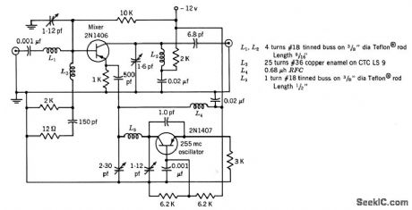
Conversion gain is 20 db and i-f output is 30 Mc.-Texas Instruments Inc. Transistor Circuit Design, McGraw-Hill, N.Y.1963, p326. (View)
View full Circuit Diagram | Comments | Reading(1115)
LOW_RANGE_OHMMETER
Published:2009/7/16 2:42:00 Author:Jessie
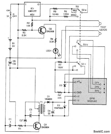
This direct-reading self-contained low-ohms meter uses the four-wire, constant-current method of resistance measurement. That eliminates any effect of test-lead resistance on measurements.
T1 is a 1:1 audio transformer, 600:600Ω. D3 is an optional Zener diode to protect the digital panel meter module DPM from excessive input voltage. The lowest reading for this circuit is 1mΩ. (View)
View full Circuit Diagram | Comments | Reading(2264)
SW_CONVERTER
Published:2009/7/13 5:24:00 Author:May

This simple circuit, built around a NE602, allows you to receive either the 6- or 9.5-MHz shortwave band on your car radio. (View)
View full Circuit Diagram | Comments | Reading(866)
SCANNING_ADAPTER
Published:2009/7/13 5:22:00 Author:May

Developed for use with 2-meter transceiver having frequency synthesizer to provide automatic scanning that is disabled when transmitting and when receiver squelch is opened by transmission on one of channels being scanned. Will hang on to channel about 5 s after scanning is disabled, to allow starting of other side of communication. Scan rate is about 250 ms per channel. U1A generates 0 output when squelch is open, producing output of 1 for U1B that disables oscillator U1C-U1D, Oscillator drives D flip-flop that turns on Q1 and Q2 alternately. When Q1 is on, LED1 is lit to indicate that secondary channel is enabled, Article covers method of increasing number of scanned channels.-B. McNair, Add-a-Scanner, 73Magazine, Nov. 1978, p 116-119. (View)
View full Circuit Diagram | Comments | Reading(745)
PREFERRED_SQUELCH
Published:2009/7/16 2:41:00 Author:Jessie

Used in sensitive receivers having agc, to suppress objectionable increase in noise output when no signal is present, as when receiving intermittent transmissions. Uses d-c amplifier that is added to grid circuit of first audio stage to bias it beyond cutoff and there by silence it until usable signal arrives.-NBS, Handbook Preferred Circuits Navy Aeronautical Electronic Equipment, Vol.1, Electron Tube Circuits, 1963, PC 64, p 64-2. (View)
View full Circuit Diagram | Comments | Reading(761)
END_OF_TRANSMISSION_BEEPER
Published:2009/7/13 5:21:00 Author:May

Release of push-to-talk (PTT) switch at end of radio conversation activates time delay for antenna changeover relay, keeping transmitter on air long enough to transmit 800-Hz tone burst indicating transmission termination. Tone is generated in simple one-transistor phase-shift oscillator powered by voltage present between PTT terminal and ground in receive mode of transceiver, which may be any voltage between 6 and 30 VDC. Transistor can be any small-signal NPN silicon with gain of at least 300 at 1 mA, such as 2N930. Parts marked with asterisk must be matched within 5%.-E. Hombostel, Automatic Beeper for Station Control, Ham Radio, Sept. 1976, p 38-39. (View)
View full Circuit Diagram | Comments | Reading(938)
FISH_SHOCKER
Published:2009/7/16 2:40:00 Author:Jessie

Two thyratrons serve as d-c interrupter that alternately connects and disconnects d-c generator from load consisting of fresh-water path between aluminum boat and aluminum grid 6 ft away. Fish swim toward positive electrode, receive shock, and are temporarily stunned. Timing circuits de. termines number and duration of pulses.-H. P. Dale, Electronic Fishing with Underwater Pulses, Electronics, 32:4, p 31-33. (View)
View full Circuit Diagram | Comments | Reading(6810)
HEADLIGHT_MONITOR
Published:2009/7/13 5:20:00 Author:May
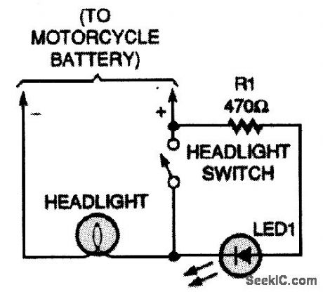
With this simple circuit, you'll never again forget to turn your headlights on. (View)
View full Circuit Diagram | Comments | Reading(760)
BRIDGE_WITH_AGC_FOR_ON_DIODE
Published:2009/7/16 2:40:00 Author:Jessie

Input signal is applied in push-pull to two diodes, then combined by two capacitors. Reduction of agc bias increases attenuation of signal by bridge.-W. A Rheinfelder, Designing Automatic Gain Control Systems, EEE, 13:1, p 53-57. (View)
View full Circuit Diagram | Comments | Reading(682)
DIODE_TR_SWITCH
Published:2009/7/13 5:19:00 Author:May

Microwave Associates MA8334 solid-state TR switch replaces conventional relays tor switching antenna back and forth between transmitter and receiver. Handles up to 50 W CW at 144 MHz, and can be used at other frequencies up to 1000 MHz by proper choice of circuit constants Measured insertion loss is 0.25 dB,and SWR is 1.23:1 when operated at 50 ohms.-T Reddeck,Solid-State VHFUHF Transmit/Receive Switch,Ham Radio,Feb1978,p 54. (View)
View full Circuit Diagram | Comments | Reading(1716)
MILLIOHM_TESTER
Published:2009/7/16 2:40:00 Author:Jessie
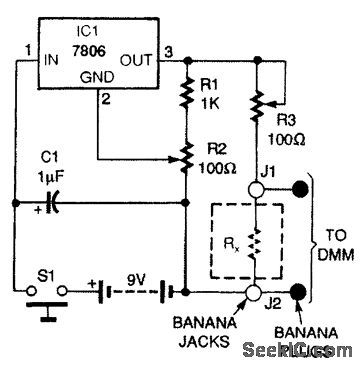
The milliohm adapter circuit is powered from a 9-V battery. A resistor to be tested (RX) is connected across banana jacks J1 and J2, and a pair of banana plugs, connected directly to J1 and J2, is plugged into the voltage input jacks of a DMM. Switch S1 applies battery power to 7806 voltage regulator IC1. Capacitor C1 removes voltage transients. Resistors R1 and R2 form a voltage divider for the GROUND pin of IC1. Potentiometer R2 trims IC1's output voltage to exactly 6 Vdc. Potentiometer R3 sets the output current through RX, to 100mA. Because R3 is a relatively large resistance compared to RX, the error introduced by different values of RX, (1 mΩ to 1Ω), the effect it will have on the 100-mA current source, is below 2 percent. (View)
View full Circuit Diagram | Comments | Reading(3209)
| Pages:693/2234 At 20681682683684685686687688689690691692693694695696697698699700Under 20 |
Circuit Categories
power supply circuit
Amplifier Circuit
Basic Circuit
LED and Light Circuit
Sensor Circuit
Signal Processing
Electrical Equipment Circuit
Control Circuit
Remote Control Circuit
A/D-D/A Converter Circuit
Audio Circuit
Measuring and Test Circuit
Communication Circuit
Computer-Related Circuit
555 Circuit
Automotive Circuit
Repairing Circuit