
Circuit Diagram
Index 603
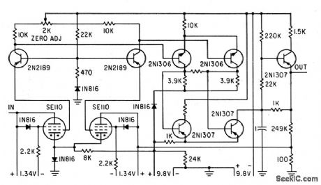
TUNNEL_DIODE_COUPLED__MICROENERGYFLIP_FLOP
Published:2009/7/14 20:56:00 Author:May

Fan-in and fan-out capabilities per unit dissipation are improved up to ten times over existing types of logic. Use of tunnel diodes allows low supply voltages, resulting in low circuit dissipation.-T. Maguire, Electro-Optical Developments Highlight NEREM, Electronics, 34:45, p 73-77. (View)
View full Circuit Diagram | Comments | Reading(585)
BUILDING_BLOCK_AMPLIFIER
Published:2009/7/14 23:42:00 Author:Jessie

Has voltage gain of 1,000 and gain-bandwidth product of 15 Mc. High-fidelity audio preamp can be designed with two such packages, one with equalization network and one with tone control network.-L. J. Sevin, Jr., Field-Effect Transistors, McGraw-Hill, N.Y., 1965, p 74. (View)
View full Circuit Diagram | Comments | Reading(698)
STRAIN_GAGE_AMPLIFIER
Published:2009/7/14 20:56:00 Author:May
Battery-powered circuit for low-impedance transducers has voltage gain up to 10,000 with low noise and low drift.-D-C Amplifier uses Solion Tetrodes, Electronics, 35:39, p108. (View)
View full Circuit Diagram | Comments | Reading(0)
SINGLE_ENDED_CLASS_B_OUTPUT
Published:2009/7/14 23:41:00 Author:Jessie

High-fidelity 10-w amplifier uses capacitor and diodes to couple class A driver,to single-ended class B output feeding 16-ohm speaker. Input stages are equalized for RIAA curve. Frequency response is flat within 1.5 db from 30 to 15,000 cps.-H.C.Lin and B.H.White,Single-Ended Amplifiers for Class B Operation Electronics,32:22,p 86-87. (View)
View full Circuit Diagram | Comments | Reading(1181)
TRIANGLE_WAVEFORM_GENERATOR
Published:2009/7/14 23:41:00 Author:Jessie

A low-frequency triangle-waveform generator is made from a single LM158 dual op amp and a few inexpensive components. The output frequency can be varied by changing the R5, Changing the value of C1, will shift the circuit's frequency range: Increasing the value will lower the oscillator's frequency and reducing the value will increase the frequency. Resistor R4 can be varied to change the output level. Powered from a 9-V supply, the circuit produces a 2-V p-p triangular output waveform. (View)
View full Circuit Diagram | Comments | Reading(971)
WIDE_TEMPERATURE_RANGE
Published:2009/7/14 20:55:00 Author:May

Gives 10-Mc op eration from -55℃ to +125℃, with 3.v dock trigger. Addition of emitter-follower will improve wove form and extend operation to +150℃.-D. Hall, Using Epitaxial Transistors in Switching and R-F Circuits, Electronics, 34:13, p 52-53. (View)
View full Circuit Diagram | Comments | Reading(596)
220_MICROSEC_PHANTASTRON_DELAY
Published:2009/7/14 23:41:00 Author:Jessie

Timing accuracy of 1% is achieved by adding temperature-correcting features to basic solid-state circuit.-S. R. Parris and D. A. Staar. Highly Accurate Phantastron Delay Circuit Electronics.33:43,P72-74 (View)
View full Circuit Diagram | Comments | Reading(600)
RTTY_FROM_SATELLITE
Published:2009/7/14 23:40:00 Author:Jessie

Developed for receiving RTTY transmitted from satellite as space-only keying. Receiver can be operated in CW or narrow-filter mode, to increase signal-to-noise ratio. Any receiver having CW filter with 400-Hz bandwidth can be used. Tune for audio output of 1 kHz. Audio is converted to varying DC voltage by envelope detector and amplified by 741 opamp that drives additional filter having high-level output for space and low-level output for mark. Slow rise and fall times of varying voltage are converted to ON/OFF keying signals by 741 used as comparator, for feeding to two-stage driver and high-voltage loop keying circuit of conventional design.-K.O. Learner and W. A. Kotras, Oscar RTTY Converter, 73 Magazine. July 1975, p 53-54. (View)
View full Circuit Diagram | Comments | Reading(1126)
10_MHz_FUNCTION_GENERATOR
Published:2009/7/14 23:39:00 Author:Jessie

This circuit is built around the MAX038 IC and can provide sine, square, and triangle waveforms from 10 Hz to 10 MHz. PC-board layout techniques suitable for 50 MHz or higher should be used for best results with this circuit. (View)
View full Circuit Diagram | Comments | Reading(3121)
BA1404_STEREO_TRANSMITTER
Published:2009/7/14 20:54:00 Author:May
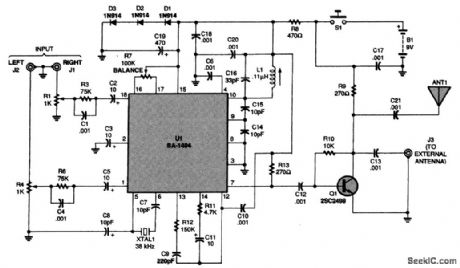
At the heart of the schematic for the FM stereo transmitter is the BA1404 FM stereo transmitter IC. Note that there is no R2 or R5 circuit.
The circuit uses the BA1404 IC (Rohm semiconductor) to implement a complete low-power FM stereo transmitter in the 88- to 92-MHz band. Line-level audio is fed to U1, the BA1404. Xtal1 is a 38-kHz crystal, and the RE oscillator tank C16/L1 (and associated components) determine RE frequency. The circuit should be carefully constructed to minimize frequency drift and microphonics. Q1 is a buffer amplifier to reduce oscillator frequency pulling. A 9-V supply is used to power the circuit. (View)
View full Circuit Diagram | Comments | Reading(6619)
6_MSEC_TO_15_SEC
Published:2009/7/14 23:38:00 Author:Jessie

Provides continuously variable delay having good settability over entire range due to use of single log-tapered pot R1.-S. G. Freshour, Wide-Range Variable Delay Circuit, EEE, 14:3, p62. (View)
View full Circuit Diagram | Comments | Reading(676)
BAR_GRAPH_READOUT_VOLTMETER
Published:2009/7/14 23:38:00 Author:Jessie
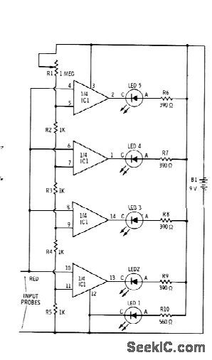
Sections of RS339 quad comparator each drive LED to give indications of four different input voltage levels, While LED 1 is connected to ground for use as zero indicator Resistors shown are for Radio Shack 276-041 red LEDs;change R6-R9 to 270 ohms and R1 to 470 ohms for green LEDs Pot R1 is used to calibrate voltage divider R2-R5 With R1 set allow resistance, comparators turn on at intervals of 1 V or more,With high resistance for R1, comparators turn on at fractional-volt intervals. –F. M. Mims,” Integrated Circuit Projects, vol. 4,” Radio Shack, Fort Worth, TX, 1977, 2 nd Ed., ρ76-85. (View)
View full Circuit Diagram | Comments | Reading(1147)
SIMPLE_PULSE_GENERATOR
Published:2009/7/14 23:37:00 Author:Jessie

Timing capacitor C1 is charged by battery B1 through R1 until Q1 is forward-biased and starts conducting. When this occurs, a forward base bias is applied to Q2 through Q1 and R3. As Q2 starts conducting, a pulse is made across collector load R6, which is coupled back to Q1's base through C2 and series resistor R5. That drives Q1 to rapidly discharge C1, and then the cycle starts over. In essence, Q1 and Q2 form a high-gain amplifiers, with C2 providing positive feedback. Diode D1 reduces C2's recovery time, while R8 establishes Q1's base bias level. Thus, it is the point at which timing capacitor C1 charges before feedback and capacitor discharge are initiated. The lower Q1's initial base bias, the higher the circuit's repetition rate. Resistor R8, therefore, serves as a frequency control, providing nine octaves of coverage. The circuit will work from 5 to 25 V, but a 9-V source is optimum. Output impedance is 600Ω. A sawtooth signal suitable for use as a linear scope sweep is available across C1. For frequency-divider, sweep-generator, and time-marker uses, synchronization pulses can be applied to Q1's base through a small capacitor. The frequency range can be shifted by using other values for C1 and C2. With values of 100μF for C1 and 3μF for C2, the circuit will work down to about 1/20 Hz. (View)
View full Circuit Diagram | Comments | Reading(1176)
1_TERAOHM_INPUT
Published:2009/7/14 23:36:00 Author:Jessie
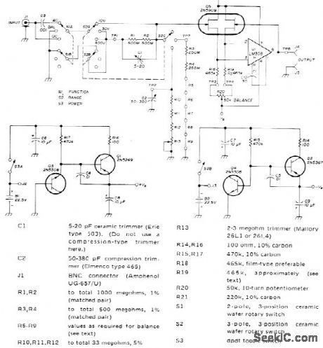
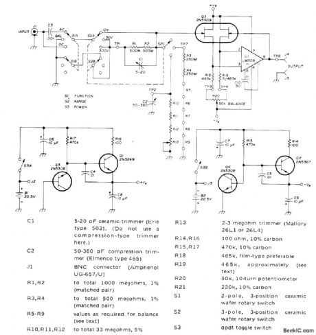
High-accuracy meter-interface amplifier for AC and DC voltage measurements has input resistance of 1,000,000 megohms. Amplifier eliminates voltmeter errors due to loading by using special 2N5909 dual FET with exceptionally low gate leakage current. FET and opamp are connected as voltage follower with gain of 1. Accuracy on 0-10 V range is 0.1% or better. For higher voltage ranges, accuracy depends on that of resistive voltage divider used. Three ranges provided have full-scale values of 10, 30, and 300 V. AC RMS inputs are limited to 70% of DC ranges. Two voltage regulators are used with battery supply to permit use of batteries exceeding 18-V voltage rating of opamp, so battery voltages can drop considerably before replacement is required. Article covers construction and adjustment.-J. R. Laughlin, High-Impedance Meter Interface, Ham Radio, Jan. 1974, p 20-25. (View)
View full Circuit Diagram | Comments | Reading(2744)
PREFERRED_PHANTASTRON_DELAY
Published:2009/7/14 23:35:00 Author:Jessie

Accepts 20 to 280V control signal, 15-V negativepulse at input 1, and 20-V positive pulse at input 2. Output is +60V, and output is -10V. R3 can be 1 to 3.3 meg and C3 100 to 1,200pf, depending on minimum and maximum duration desired.-NBS, Handbook Preferred Circuits Navy Aeronautical Electronic Equipment, Vol. I, Electron Tube Circuits, 1963 PC 56, p56-2. (View)
View full Circuit Diagram | Comments | Reading(533)
INPUT_CHANGE_RATE_TRIGGERED_RELAY
Published:2009/7/14 20:53:00 Author:May

Sensitive and stable d-c amplifier operates relay only on rapid changes of input voltage, yet is immune lo drift. Will also operate on ac signal, which is the some as rapidly changing d-c signal-Rate Circuit, Electronic Circuit Design Handbook, Mactier Pub. Corp. N.Y.1965, p239. (View)
View full Circuit Diagram | Comments | Reading(731)
CODED_LOCK
Published:2009/7/14 23:33:00 Author:Jessie

Five-digit combination lock uses five low-cost ICs operating from 5-V supply that can be derived from 12-V auto battery as shown in inset. Six set/reset bistable circuits are formed by cross-coupling pairs of dual-input NAND gates, so 0-V input is needed to change state of each. Five of bistables serve for combination, and sixth prevents operation by number in incorrect sequence. After S1 is set to one number of code, S2 is pushed to enter that number, with process being repeated for other four numbers of combination. Final correct number sets B5 and turns on Tr1, to operate relay that can be used to open door.-S. Lamb, Simple Code-Operated Switch or Combination Lock, Wireless World, June 1974, p 196.
(View)
View full Circuit Diagram | Comments | Reading(1277)
12_V_MONITOR
Published:2009/7/14 20:52:00 Author:May
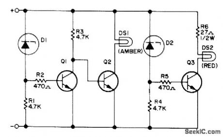
Voltage-limit sensor gives visual indication that voltage in auto or boat electric system is satisfactory for operation of critical electronic equipment. Combination of zener diodes D1 and D2 acting with base-emitter voltage drops of Q1 and Q3 makes any voltage less than 13.5 V turn on amber No. 330 pilot lamp (14 V at 80 mA), while voltage above 15.2 V turns on red pilot lamp of same type. Transistors are Motorola MPS 3704. D1is 1N5243B 13V zener, and D2 is 1N5245B 15-V zener.-M. J. Moss, Voltage Limit Sensor, 73Magazine, May 1973, p 53-54. (View)
View full Circuit Diagram | Comments | Reading(873)
DESIRED_WAVEFORM_GENERATOR
Published:2009/7/14 23:33:00 Author:Jessie

This is a filtered step-function generator in which the wave amplitude at each step is set by a linear potentiometer (R1to R4).With the potentiometers arranged in time order and side by side (the way they are in a graphic equalizer), the positions of the knobs describe the output waveform. The 555 oscillator, controlled by R5 and C0 or C2, sets the duration of each step, and (there-fore) also the wave frequency. Potentiometer R5 controls the step frequency and the capacitors define the frequency range. The output of the 555 is applied to the clock input for the 4017 decimal counter, which activates its outputs one at a time. The linear potentiometers divide the voltage of each output, and thus determine the output voltage at a given step point. The schematic shows potentiometers only in Q0, Q3, Q6, and Q9, but for smoother waveforms potentiometers should be at all of the outputs, except the CARRY-OUT pin. The composite waveform is now purified by the filter formed by R13, C4, and C5, so the output will be rounded. The amplitude is controlled by the LM386 audio amplifier's input. For high frequencies, replace the amplifier with a 741 or some other high-frequency op amp. (View)
View full Circuit Diagram | Comments | Reading(1465)
12_V_OVERVOLTAGE_LIMITER
Published:2009/7/14 23:31:00 Author:Jessie

Single LM111 comparator is basis for simple overvoltage protection of circuits drawing less than 50mA. Fraction of input supply is compared to 1.2-V reference. When input exceeds reference level, power is removed from output.-R. C. Dobkin, Comparators Can Do More than Just Compare, EDN Magazine, Nov. 1, 1972, p 34-37. (View)
View full Circuit Diagram | Comments | Reading(942)
| Pages:603/2234 At 20601602603604605606607608609610611612613614615616617618619620Under 20 |
Circuit Categories
power supply circuit
Amplifier Circuit
Basic Circuit
LED and Light Circuit
Sensor Circuit
Signal Processing
Electrical Equipment Circuit
Control Circuit
Remote Control Circuit
A/D-D/A Converter Circuit
Audio Circuit
Measuring and Test Circuit
Communication Circuit
Computer-Related Circuit
555 Circuit
Automotive Circuit
Repairing Circuit