
Circuit Diagram
Index 608
CHOPPER_TYPE_DATA_AMPLIFIER
Published:2009/7/14 20:33:00 Author:May
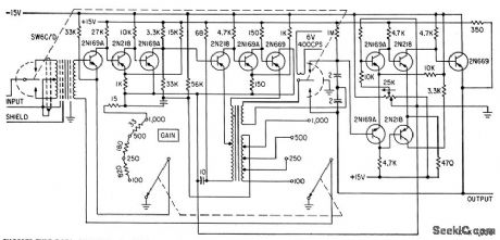
Careful design of transistor circuits between chopper input and chopper output gives gain stability within 0.01% for long-term operation (1,000 hours) front 15 to 35 C, linearity is equally precise for normal output range of plus or minus 10V.-F. Offner, Transistorized Data Amplifier Has High Gain-Stability, Electronics, 33:27, p 55-57. (View)
View full Circuit Diagram | Comments | Reading(797)
VOLTAGE_CONTROLLED_CRYSTAL
Published:2009/7/14 20:33:00 Author:May

Voltage-variable capacitance tuning diode in series with crystal feedback path of Motorola MC10116 IC gives frequency deviation of about ±50 PPM for 1-MHz crystal when using tuning voltage range of 0-25 VDC. Deviation is greater at higher crystal frequencies.-B. Blood, IC Crystal Con-trolled Oscillators, Motorola, Phoenix, AZ, 1977, AN-417B, p 6.
(View)
View full Circuit Diagram | Comments | Reading(1393)
TUNING_BY_REACTANCE_SWITCHING
Published:2009/7/14 20:31:00 Author:May

Tuning voltage V, in range of 0 to 7 V changes effective capacitance during peak positive portion of collector voltage cycle, to provide tuning over range of about 90 to 150 MHz. Reactance-switching HP 5082-3188 diode CR1 switches in additional capacitance for oscillator using Motorola 2N5208 transistors.-C. Weber, VCO Reactance Switching Provides Broad Tuning Range, EDN Magazine, March 20, 1977, p 151 and 153. (View)
View full Circuit Diagram | Comments | Reading(674)
BOOTSTRAP_FET
Published:2009/7/15 2:00:00 Author:Jessie

Input impedance is high at low frequencies (180 meg at 10 cps), butdrops to 3 meg at 10 kc. High collector current contributes to high over-all noiselevel.-B. Smith, Low. Noise FETs Sound Good To Circuit Designers, Electronics, 37:31,p 58-62. (View)
View full Circuit Diagram | Comments | Reading(1250)
FSK_FOR_NRZ_INPUT
Published:2009/7/15 1:59:00 Author:Jessie

Crystal-controlled frequency-shift keyer accepts nonreturn-to-zero digital input and generates 5-V P-P FSK output signal having less than 3% total harmonic distortion, at standard 2.125- and 2.975-kHz radio-teletype frequencies. When input is low, counter A divides by seven; for high or logic 1 input, counter divides by five. Counter B divides by eight to produce required output frequencies. EXCLUSIVE-OR gates G1 and G2 generate fist approximation to desired sine-wave out-put, for filtering by three-pole active Butter-worth low-pass filter having 4.75-kHz cutoff.-K. Erickson, Frequency4hift Keyer Features Rock-Steady Operation, EDN Magazine, Jan. 5, 1977, p 44. (View)
View full Circuit Diagram | Comments | Reading(643)
BALANCING_D_C_AMPLIFIER
Published:2009/7/14 20:21:00 Author:May
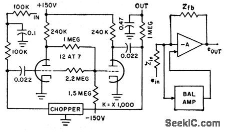
Gain is 300.Detects slow changes al summing point of operational amplifier, amplifies drift voltage, and provides opposite-polarity output signal for second input grid of operational amplifier, much as in null-seeking servomechanism.-L.S. Klivans, D-C Amplifiers for Control Systems, Electronics, 31:47, p96-100. (View)
View full Circuit Diagram | Comments | Reading(696)
BIPOLAR_PULSE_TRAINS
Published:2009/7/15 1:58:00 Author:Jessie

Output of Signeties 555 timer F, consisting of unipolar waveform varying from ground to +5 V, is converted to bipolar pulse train having duration equal to that of output pulse from lower 555 timer. While P is high, comparator 2 is on, forcing R2 to ground and placing base of Q1 at 2.5 V (because comparator 1 is off, forcing R1, high). Comparator 2 goes off when timer P goes low, and action of comparator 1 is turned on and off by timer F to produce bipolar pulse train at E0.-G. L. Assard, Derive Bipolar Pulses from a Unipolar Source, EDN Magazine, April 5, 1977, p 144. (View)
View full Circuit Diagram | Comments | Reading(982)
FET_SAMPLE_HOLD_D_C_AMPLIFIER
Published:2009/7/14 20:19:00 Author:May

Has low output impedance for rapid charging of sampling capacitor, unity gain, and no d-c offset adjustment period.-L. J. Sevin, Jr., Field-Effect Transistors, McGraw-Hill, N.Y., 1965,p114. (View)
View full Circuit Diagram | Comments | Reading(715)
AFSK_GENERATOR
Published:2009/7/15 1:58:00 Author:Jessie

Uses phase-continuous frequency shift to prevent out-of-band transients while generating radio frequencies of 1450 and 1620 Hz. Second harmonic is outside passband of modern SSB equipment. Frequency of sine wave is determined by C1 and total resistance connected to pin 7 or 8 of Exar XR2206.-E. Kirchner, Serial Converter for 8-Level Teleprinters, Ham Radio, Aug. 1977, p 67-73. (View)
View full Circuit Diagram | Comments | Reading(849)
TOUCH_SWITCH_Ⅲ
Published:2009/7/14 20:14:00 Author:May

The touch switch shown uses 9-Vdc operation, rather than the commonly used 120-Vac. (View)
View full Circuit Diagram | Comments | Reading(706)
VARIABLE_GAIN_INVERTER_AMPLIFIER
Published:2009/7/15 1:58:00 Author:Jessie

Gives gain variations of up to 10 to1, with less than 10% harmonic distortion at 1 v output through use of tetrode transistor, to provide precise voltage regulation of output of d-c to 400-cps a-c inverter. Error current from d-c amplifier of inverter is applied to base 2 of 04, causing ac voltage gain of stage to vary with magnitude of error current..-R.. Wileman, linear Circuits Regulate Solid-State Inverter, Electronics, 33:16, p 61-63. (View)
View full Circuit Diagram | Comments | Reading(682)
NONPRECISE_PHANTASTRON_VARIABLE_DELAY
Published:2009/7/15 1:58:00 Author:Jessie

Used to delay beginning of crt sweep for expanded display. Provides three ranges: 0 to 5, 60, and 200 miles. Circuit is basically cathode-coupled phantastron, with additional coupling by returning suppressor and screen to same divider. Cathode follower reduces recovery time and provides low-impedance point for range switching.-NBS, Handbook Preferred Circuits Navy Aeronautical Electronic Equipment, Vol. 1, Electron Tube Circuits, 1963, p N9-3. (View)
View full Circuit Diagram | Comments | Reading(740)
SIMPLE_TOUCH_SWITCH
Published:2009/7/14 20:13:00 Author:May

This circuit has two high-gain transistors. Operation occurs when the ambient 60-Hz ac field is impressed on the touch pad during the finger contact. The signal turns on Q1, causing Q2 to energize the relay. Capacitor C1 is used to prevent the relay from oscillating. (View)
View full Circuit Diagram | Comments | Reading(0)
CAPACITOR_MIKE_PREAMP
Published:2009/7/15 1:57:00 Author:Jessie

Fet provides required high input impedance. Can easily bemounted in microphone. Emitter-follower with output impedance of about 100 ohms willdrive 500 feet of microphone cable without appreciably affecting frequencyresponse.-L.J. Sevin, Jr., Field-Effect Transistors, McGraw-Hill, N.Y., 1965, p 75. (View)
View full Circuit Diagram | Comments | Reading(1032)
GENERATOR_FOR_170_Hz_SHIFT
Published:2009/7/15 1:56:00 Author:Jessie

Provides precise 2125- and 2295-Hz audio tones without requiring counter to establish correct frequency, Used for adjusting AFSK oscillator, Crystal can be 459.259 kHz (channel 48), which with appropriate divider chains gives output frequencies accurate within 2 Hz while preserving 170-Hz relative shift within 0.1 Hz. For even greater ac-curacy, order crystal that has been adjusted to exactly 459.000 kHz. When input is grounded, divide ratio is 25 to give 2295 Hz. When input is high, divide ratio is 27 to give 2125 Hz. Pin 11 of U1-U4 and pin 7 of U5 are grounded.-H. Nurse, Crystal Controlled AFSK Generator, Ham Radio, Dec. 1973, p 14-17.
(View)
View full Circuit Diagram | Comments | Reading(954)
ALTERNATIVE_LIGHT_OPERATED_TURNOFF_TOUCH_SWITCH
Published:2009/7/14 20:11:00 Author:May

When the touch plate is touched, it turns the output of IC1 on, giving a positive potential to the base of Q2. In turn, that turns on pins 4, 5, and 6 of IC2, triggering the SCR's gate and energizing RY1.When RY1 is energized, its contacts pull in, turning on the ac bulb. When R1 is hit by a strong light, it turns on the SCR and energizes RY1. To turn the ac bulb off, just point a strong flashlight at R2; this decreases the base resistance of Q3, making its base positive and, therefore, energizing RY2. When the contact of RY2 pulls in, it disconnects the anode of the SCR from the positive supply, turning it off. Or you can press S2 to energize RY2 and turn off the ac bulb (View)
View full Circuit Diagram | Comments | Reading(1527)
LM322_ASTABLE
Published:2009/7/15 1:55:00 Author:Jessie

National LM322 timer generates narrow negative pulse whose width is approximately 2RC seconds. VCC is 4.5-20 V. Will drive loads up to 5mA. -H. M. Berlin, IC Timer Review, 73Magazine, Jan. 1978, p 40-45. (View)
View full Circuit Diagram | Comments | Reading(1075)
BANDPASS_FOB_85O_Hz_RTTY_SHIFT
Published:2009/7/15 1:55:00 Author:Jessie

Three-stage active Butterworth input filter passes 2125- and 2975-Hz tones plus modulation side-bands and allowance for drift in RTTY receiver. Inset shows how 741 opamps are biased when used with single power supply. Article gives step-by-step design and alignment procedures.-P. A. Stark, Design an Active RITY Filter, 73 Magazine, Sept. 1977, p 38.-43. (View)
View full Circuit Diagram | Comments | Reading(1052)
FET_PNP_DARLI_NGTON
Published:2009/7/15 1:55:00 Author:Jessie


P-channel fet is combined with pnp transistor in equivalent to Darlington connection, for use with high-input-impedance low-frequency transducers.Spot noise figure is 7 db at 10 cps and 3 db at 100 cps. Broadband noise figure from10 cps to 10 kc is 1.7 db with 200K generator resistance.-Texas Instruments Inc., Solid-State Communications, McGraw-Hill, N.Y., 1966, p 136. (View)
View full Circuit Diagram | Comments | Reading(1327)
SWITCH_OPERATED_TURNOFF_TOUCH_SWITCH
Published:2009/7/14 20:08:00 Author:May

When S1 is closed,the circuitry is on in standby mode.When the touch plate is touched,the output of the 555 time IC1 goes high,supplying a positive potential to the base of transistor Q2,aiding its bias,The transistor is then on,allowing current to flow through pin4,5 and 6 of IC2.The gate of the SCR is then triggered,the relay is energized,and its contacts turn the ac bulb on.To turn the bulb off,just press S2(RESET),which disconnects the ande of the SCR from the positive supply,turning it off and deenergizing the relay,The light-dependent resistor(R7)is used if you want to turn on the circuit remotely.Just point a flashinght at R7 to decrease its resistance,leaving only the 1000Ω resistor as the base resistance.The resistance give the base a positive positive potential,forward biasing the emitter-base junction of transistor Q1.Transistor Q2 is also turned on because its base is made positive by Q1,which triggers SCR1,energizing the relay.
(View)
View full Circuit Diagram | Comments | Reading(1323)
| Pages:608/2234 At 20601602603604605606607608609610611612613614615616617618619620Under 20 |
Circuit Categories
power supply circuit
Amplifier Circuit
Basic Circuit
LED and Light Circuit
Sensor Circuit
Signal Processing
Electrical Equipment Circuit
Control Circuit
Remote Control Circuit
A/D-D/A Converter Circuit
Audio Circuit
Measuring and Test Circuit
Communication Circuit
Computer-Related Circuit
555 Circuit
Automotive Circuit
Repairing Circuit