
Circuit Diagram
Index 607
STEREO_MULTIPLEX_TUNER
Published:2009/7/14 22:57:00 Author:Jessie

Consists of demodulator D1-D2, 19-38 kc doubler Q3 19-kc amplifier Q2, composite amplifier Q2, and stereo station indicator Q4 with lamp. Diodes are 1N60. Uses lime-share method that eliminates need for 15.kc low-pass fiber and 23-53 kc bandpass filter.-R. Brubaker, A Low Cost All Solid-Slate FM Stereo Multiplex System, Motorola Application Note AN-207, Mar. 1966. (View)
View full Circuit Diagram | Comments | Reading(825)
45_kHz_LOW_PASS_STATE_VARIABLE_FILTER
Published:2009/7/14 20:39:00 Author:May

Used In precision telephone-network active equalizer Camping value is 0.082, which requires 1% components. For high pass, take out-put from first opamp; for band pass, take output from second opamp.-D. Lancaster, Active-Filter Cookbook, Howard W Sams, Indianapolis, IN, 1975, p 147. (View)
View full Circuit Diagram | Comments | Reading(1605)
TAPE_MICROPHONE_PREAMP
Published:2009/7/14 22:54:00 Author:Jessie

Uses silicon planer npn transistors, making it necessary to have temperature-compensating resistor in emitter circuit of first stage. Noiselevel is 66 db below reference level output with weighted measurement. Frequencyresponse is fiat within 0.25 db from 30 cps to 15 kc, and total harmonic distortionis 0.01% at 1.2 v output.- Transistor Manual, Seventh Edition, General ElectricCo., 1964, p 256. (View)
View full Circuit Diagram | Comments | Reading(818)
TTY_RESETS_CPU
Published:2009/7/14 22:54:00 Author:Jessie

Circuit uses break key on TTY as reset button for microprocessor. Retrig-gerable mono IC1 monitors data input line from TTY, which goes low for spacing condition. During normal data input, constant spacing pulses in data retrigger mono, keeping IC2 reset. When break key is depressed, input data goes to steady space and IC1 times out. IC2 then transfers high on its data input to its output to produce reset signal for CPU. Values of R2 and C1 give 150-ms period for mono, suitable for baud rates of 110 and higher,-C. Sondgeroth, Reset Your CPU from Your TTY's Break Key, EDN Magazine, May 5, 1978, p 39. (View)
View full Circuit Diagram | Comments | Reading(712)
FREEZER_FAILUREALARM
Published:2009/7/14 22:54:00 Author:Jessie

Loudspeaker is energized by 4011 audio oscillator and 2N2222 transistor operating from 9-V battery when ice melts and allows permanent magnet to drop on reed switch and close it. Magnet is bonded to wall inside of freezer with mixture of antifreeze and water.-J. A. Sandier, 11 Projects under $11, Modern Electronics, June 1978, p 54-58. (View)
View full Circuit Diagram | Comments | Reading(1006)
LOW_VOLTAGE_ALARM_1
Published:2009/7/14 22:53:00 Author:Jessie

Simple indicator circuit uses hex inverter IC to monitor several different input voltages. Technique is flexible and easily modified for different voltage values (either positive or negative) and additional in-puts. When negative input (V1, V2, or V3) falls below breakdown voltage of its zener, logic 0 appears at inverter output (at wired-OR connection). Because lamp-driving inverter has logic 0 at its input, lamp goes out as no-go signal. When positive input V4 falls below predetermined value, logic 0 again causes no-go indication,-R. J. Buonocore, Under-Voltage Sensing Circuit, EDN/EEE Magazine, Dee. 1, 1971, p 48-49. (View)
View full Circuit Diagram | Comments | Reading(721)
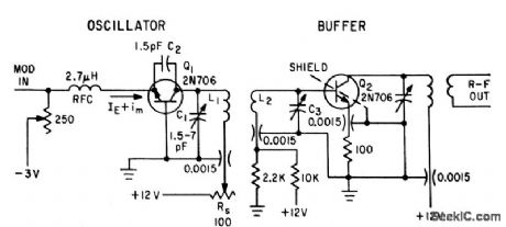
VARACTOR_MODULATES_24_MC_F_M_OSCILLATOR
Published:2009/7/14 22:53:00 Author:Jessie

Modulating signal is applied to vat deviation of 60 kc.-N. Downs and B. varactor diode in frequency-determining circuit of telemetering oscillator. Linearity is 2% for deviation of 60 kc.-N. Downs and B. van Sutphin, Solid-State Transmitter Ready for UHF Telemetry, Electronics, 37:17, p 76-80. (View)
View full Circuit Diagram | Comments | Reading(730)
15_25_kHz_SINE_WAVE
Published:2009/7/14 20:38:00 Author:May

Three-section phase-shift oscillator is linear over its frequency range and has good sine waveform. Phase-shifting 2.5k network is included in feedback loop of amplifier to give voltage-controlled oscillator action.- Low Frequency Applications of Field-Effect Transistors, Motorola, Phoenix, AZ, 1976, AN-511A, p 8. (View)
View full Circuit Diagram | Comments | Reading(807)
60_DB_LOW_NOISE_FET_AMPLIFIER
Published:2009/7/14 22:52:00 Author:Jessie

Gives maximum voltage gain of 60 db, constant within 0.5 db from -55 to +125℃ with built-in gain adjustment. Has good low-frequency response, along with extremely low noise, as little as 5 db at 10 cps. Used with low-level transducers, null detectors, recorders, oscilloscopes, and medical research equipment.-Texas Instruments Inc., Solid-State Communications, McGraw-Hill, N.Y., 1966, p 293. (View)
View full Circuit Diagram | Comments | Reading(834)
52_MHz_WITH_VVC_FM
Published:2009/7/14 20:37:00 Author:May


Voltage-variable capacitor CO rovides ±75 kHz modulation of basic 52-MHz transistor oscillator operating from 15-V supply. Modulation linearity is good for voltage inputs up to ±200 mV, making circuit suitable for commercial FM use.- FM Modulation Capabilities of Epicap VVC's, Motorola, Phoenix, AZ, 1973, AN-210, p 2. (View)
View full Circuit Diagram | Comments | Reading(680)
INSTANT_ULTIMATE_VALUE
Published:2009/7/14 22:51:00 Author:Jessie

Circuit instantly computes ultimate value of logarithmically in-creasing input signal Ei y performing augmented differentiation that gives step function equal to ultimate value EU, Uses Optical Electronics 9406 opamp. Circuit values are computed from EU = EO = -R2EjR1 – R2Cdej/dt.- Derivative Circuit Indicates Ultimate Value Instantly, Optical Electronics, Tucson, AZ, Application Tip 10179.
(View)
View full Circuit Diagram | Comments | Reading(730)
SELF_REACTANCE_MODULATION
Published:2009/7/14 22:51:00 Author:Jessie
Modulation current injected at emitter changes collector-base voltage, thus varying output capacitance, tank resonant frequency, and oscillator frequency +or 230-Mc pam/f-m telemetery beacon.-T. M. Conrad, Self-Reactance Modulation in Telemetry Oscillators, Electronics, 35:9, p 35-37. (View)
View full Circuit Diagram | Comments | Reading(1229)
HLTRAHIGH_IMPEDANCE_AMPLIFIER
Published:2009/7/14 20:36:00 Author:May
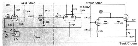
Bridge balanced series-compensated d-c amplifier using ordinary vacuum tubes gives input impedance of 250,000 meg. For precise voltage measurements without loading high-impedance circuits,-J. Morrison. For precise Measurements An Ultrahigh Impedance Amplifier. Electronics.35:40,p49 (View)
View full Circuit Diagram | Comments | Reading(670)
200_MC_VOLTAGE_CONTROLLED_OSCILLATOR
Published:2009/7/14 22:50:00 Author:Jessie

Uses two tunnel-diodes in astable mvbr to give symmetrical square wave output. Used to produce wide frequency swing with respect to center frequency, linearly, when small control voltage is applied.-F. H. Lefrak, Tunnel-Diode Oscillator Expands F.M System's Tunnel-Diode Oscillator Expands F-M System's Channel Capacity, Electronics ,39:1, P 105-109. (View)
View full Circuit Diagram | Comments | Reading(783)
AFSK_SHIFTS_UP_TO_20_kHz
Published:2009/7/14 22:50:00 Author:Jessie

Wide-range generator can be tuned from 50 Hz to 20 kHz, for shifting between two frequencies as much as 20 kHz apart. UI is 555 timer connected as astable MVBR. When Q3 is biased off, charge/discharge currents for C1 flow chiefly through R1 and R2 to determine lower frequency of oscillation, When Q3 is on, R2 is effectively shorted and frequency is increased.Q1 acts as buffer and inverter so higher voltage at input gives higher tone. Keying occurs when input voltage exceeds 1 V with 5-V supply. If 10K supply resistor for al is reduced to 1000 ohms, keying voltage increases to 3V.-T. M. Whittaker, Wide-Range AFSK Generator, QST, May 1977, p 48. (View)
View full Circuit Diagram | Comments | Reading(970)
VOLTAGE_TO_FREQUENCY_CONVERTER
Published:2009/7/14 22:50:00 Author:Jessie
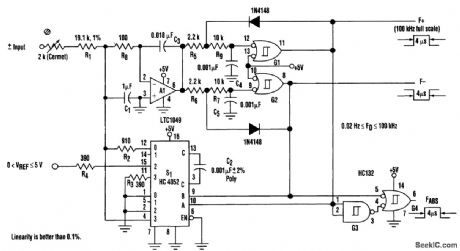
The voltage-to-frequency converter draws <10 mA from one +5-V supply while producing three 0- to 100-kHz pulse outputs.One output is proportional to positive input voltages and inactive for negative inputs, another responds when the input is negative, and a third outputs a frequency that is proportional to the input's absolute value. The converter's unadjusted zero offset is less than 1 ppm of full scale and its linearity is better than 0.1 percent. (View)
View full Circuit Diagram | Comments | Reading(0)
555_TRIGGER
Published:2009/7/14 22:49:00 Author:Jessie
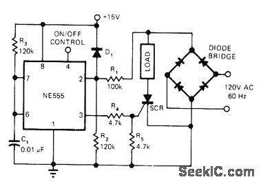
Low-cost 555 timer provides ON/OFF and proportional-control switching of AC loads without generating RFI or voltage spikes. Timer is used in monostable mode, retriggering every half-cycle when voltage at pin 2 falls below about 1.67 V. R3 and C1 fix pulse width at about n ms, long enough to ensure firing SCR in next half-cycle yet short enough to turn SCR off at next zero-crossing without timing-cycle pulse. Pin 4 serves as ON/OFF control input. Varying duty cycle of square wave here gives proportional control for heating and other uses.-M, E, Anglin, Low Cost Zero-Cross Thyristor Trigger Uses a 555 IC, EDN Magazine, Sept. 5, 1977, p 180-181. (View)
View full Circuit Diagram | Comments | Reading(4997)
TOUCH_TONE_ENCODER_1
Published:2009/7/14 20:36:00 Author:May

Consists of SME Touch-Tone generator and keyboard made by Data Signal (Albany, GA) mounted on any small transistor radio. Only audio section is used, with output tones from loudspeaker being fed acoustically to microphone of FM amateur station. Article gives construction details,-D. In-gram, The Shirt Pocket Touch-Tone, 73 Magazine, Nov. 1976, p 58-59. (View)
View full Circuit Diagram | Comments | Reading(973)
FET_OPERATIONAL_AMPLIFIER
Published:2009/7/14 20:35:00 Author:May


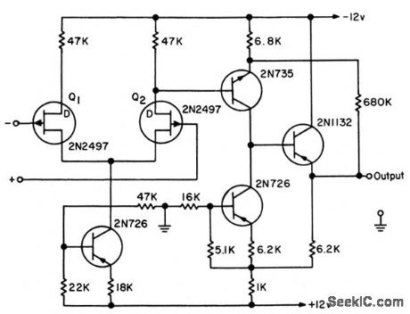
Open-loop voltage gain at direct current is above 100,000. When operated open-loop, makes excellent voltage comparator having high resolution.-L. J. Sevin, Jr. Field-Effect Transistors, McGraw-Hill, N.Y. 1965, p107. (View)
View full Circuit Diagram | Comments | Reading(1211)
FAST_SLEW_VCO_DRIVER
Published:2009/7/14 20:34:00 Author:May

High-performance circuit slews at 4000 V/μs when operating from 80-V supply and provides output levels up to +30 VDC. Circuit handles large-signal modulation rates up to 20 MHz for 60-V varactors and small-signal bandwidths up to 86 MHz. Input opamp can be M. S. Kennedy Model 770 or other fast-input unit having -6 dB per octave rolloff. Operation in transimpedance configuration means associated buffer amplifier can have high gain. RE is 250 ohms, R1 is 100, R3 is 4.3K, R5 is 170, and R8 is 90.-H. Bunin, Low Cost VCO Driver Amplifiers Really Perform lf Designed Right, EDN Magazine, Oct. 5, 1974, p 51-55.
(View)
View full Circuit Diagram | Comments | Reading(849)
| Pages:607/2234 At 20601602603604605606607608609610611612613614615616617618619620Under 20 |
Circuit Categories
power supply circuit
Amplifier Circuit
Basic Circuit
LED and Light Circuit
Sensor Circuit
Signal Processing
Electrical Equipment Circuit
Control Circuit
Remote Control Circuit
A/D-D/A Converter Circuit
Audio Circuit
Measuring and Test Circuit
Communication Circuit
Computer-Related Circuit
555 Circuit
Automotive Circuit
Repairing Circuit