
Circuit Diagram
Index 621
IC_MODERNIZES_VTVM
Published:2009/7/15 2:10:00 Author:Jessie

LM310H voltage-follower IC converts VTVM into battery-operated IC voltmeter. Input impedance and scale accuracy are unchanged. Conversion shown is for Heathkit IM-11 VTVM but will apply to most other VTVMs. Semiconductor diodes CR100 and CR101 replace original 6AL5 detector and LM310H high-impedance unity-gain voltage follower replaces original 12AU7. C105 and C106 bypass battery supply and should be connected directly to U100. CR102 and CR103 provide overvoltage protection.-M. Kaufman, How to Convert Your VTVM to an IC Voltmeter, Ham Radio, Dec. 1974, p 42-44. (View)
View full Circuit Diagram | Comments | Reading(2088)
TEMPERATURE_SHIFT_CIRCUIT
Published:2009/7/14 4:43:00 Author:May

The temperature-shift meter is designed to detect small changes in temperature, rather than give exact temperature levels. (View)
View full Circuit Diagram | Comments | Reading(590)
UNDERWATER_PREAMPLIFIER
Published:2009/7/15 2:09:00 Author:Jessie
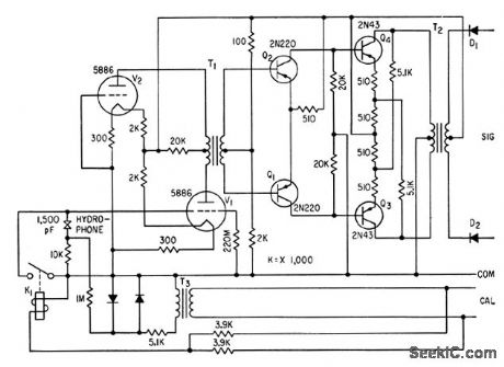
Used in package with hydrophone for measuring ambient oceannoise over periods of months, as one basis for sonar system design. Output is fedthrough cable pair to shore installation.-J.V. Schaefer, Remote Preamplifiers forUnder Ocean Work, Electronics, 33:28, p 60-62. (View)
View full Circuit Diagram | Comments | Reading(641)
STABILIZED_MULTI_INPUT_AUDIO_PREAMP
Published:2009/7/15 2:07:00 Author:Jessie
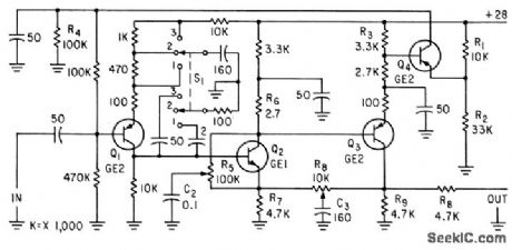

Switch gives choice of input impedance, frequency response, and level-compensation network. R5 is tone control. Q4 Provides biascurrent to base of Q1 for stabilization-H.W. Parmer, Two Easy Ways to Stabilize Power -Transistor Hi-fi Amplifiers, Electronics,35:43,p 56-58. (View)
View full Circuit Diagram | Comments | Reading(885)
FAST_RECOVERY
Published:2009/7/15 2:07:00 Author:Jessie

Addition of C2 to basic circuit reduced recovery time from 2 microsec to 0.5 microsec. Used in computers.-L. C. Radzik and J. J. Curtis, Adding A Component Reduces Recovery Time. Electronics.38:2,p78-79 (View)
View full Circuit Diagram | Comments | Reading(591)
POWER_TRANSISTOR_DISSIPATION
Published:2009/7/14 5:36:00 Author:May

Circuit protects power transistors in various combinations without limiting capabilities of AF amplifier when driving reactive loudspeaker load. With continuous signal drive into normal load, R1 draws current from C1 through D1, in opposition to R5. This gives drops of about 0.12 V across C1 and C2, allowing full drive. With short-circuited load, however, capacitor drops increase to about 0.55 V, thereby limiting average current in each output transistor to about 1.1 A. Diodes D5 and D6 are not critical, and simply prevent current flow from base to collector of transistors. -M. G. Hall, Amplifier Output Protection, Wireless World, Jan. 1977, p 78.
(View)
View full Circuit Diagram | Comments | Reading(769)
5_min_AC_TIMER
Published:2009/7/14 5:36:00 Author:May

This 555-based circuit will power a load for up to 5 minutes, depending on the setting of R1. Note the transformerless power supply made up of C1, C2, D1, and D2. The timer covers 0 to 5 minutes, or a little more, by measuring the time needed to charge C3 through R1, which is adjustable. To switch the ac power to the load, the timer uses a triac (a solid-state ac switch) instead of a relay. In the power supply, the capacitive reactance of C1 limits the current without generating heat. Use a metal-film capacitor for C1, not an electrolytic. Be sure to observe the voltage rating-use a capacitor rated for at least 200 V (preferably 600 V). Zener diode D1 limits the voltage, and D2 and C2 are the rectifier and filter. (View)
View full Circuit Diagram | Comments | Reading(3351)
MICROPHONE_PREAMP
Published:2009/7/14 5:35:00 Author:May

Used in high-quality stereo cassette deck operating from AC line or battery. Provides three preset gain positions (10, 33, and 100) to meet amplification requirements of practically all types of microphones used with tape recorders. Recording input of cassette deck provides only enough gain for re-cording from audio amplifier or radio tuner delivering 50-100 mV at fairly low impedance, hence is not suitable for microphone input. Article gives all other circuits of cassette deck and describes operation in detail.-J. L. Linsley Hood, Low-Noise, Low-Cost Cassette Deck, Wireless World, Part 2-June 1976, p 62-66 (Part 1-May 1976, p 36-40; Part 3-Aug. 1976, p 55-56l. (View)
View full Circuit Diagram | Comments | Reading(1470)
PLAYBACK_PREAMP
Published:2009/7/14 5:34:00 Author:May
Circuit is optimized for automotive use at supply of 10-15V. Wideband 0-dB reference gain is 46 dB. NAB equalization is included. Tape speeds can be 1 7/8 or 3 3/4 in/s.- Audio Handbook, National Semiconductor, Santa Clara, CA, 1977, p 2-31-2-37. (View)
View full Circuit Diagram | Comments | Reading(747)
VARIABLE_DUTY_CYCLE_TIMER
Published:2009/7/14 5:33:00 Author:May

This NE555 circuit produces a variable duty-cycle output. (View)
View full Circuit Diagram | Comments | Reading(0)
RECORDING_AMPLIFIER_1
Published:2009/7/14 5:33:00 Author:May

Designed for use with microphone having 10-mV peak output and recording head requiring 30-μA AC drive current. Output swing is 6 VRMS. High-frequency cutoff is 16 kHz, with circuit designed for slope of 6 dB per octave between 4 kHz and 16 kHz to compensate for falling frequency response of recording head starting at 4 kHz.- Audio Handbook, National Semiconductor, Santa Clara, CA, 1977, p 2-31-2-37. (View)
View full Circuit Diagram | Comments | Reading(703)
CROWBAR
Published:2009/7/14 5:32:00 Author:May

When output of regulator for microprocessor power supply exceeds maximum safe voltage as determined by zener Q1, SCR Q2 is triggered on and conducts heavily, blowing fuse rapidly to protect equipment. Fuse rating is 125% of nominal load. Choose SCR to meet voltage and current requirements. Choose zener for desired trip voltage. Each germanium diode in series with Q1 will add 0.3 V to trip voltage, and silicon diodes add 0.6 V. To calibrate, place 1K resistor temporarily in series with Q2 and measure drop across it to see if SCR fires and produces surge on meter at desired VCC.-J. Starr, Want to Buy a Little Insurance? , Kilobaud, 0ct. 1978, p 89. (View)
View full Circuit Diagram | Comments | Reading(0)
RECORDING_AMPLIFIER
Published:2009/7/14 5:32:00 Author:May

Used in high-quality stereo cassette deck operating from AC line or battery. Uses active RC circuit R16-R17-C12-C13-R19-VR2-C15 to provide required high-frequency recording characteristic for use with Garrard CT4 recording head; component values may have to be changed for other heads. C18 (3.9 nF) is switched in to change from basic 70-μs recording characteristic to 120μs. C17 and R27 provide new cassette-standard bass preemphasis at 3,180μs. Recording level is chosen as 0 VU at 660 Hz. Output feeds VU meter through silicon diode, Article gives all other circuits of cassette deck and describes operation in detail.-J. L. Linsley Hood, Low-Noise, Low-Cost Cassette Deck, Wireless World, Part 1-May 1976, p 36-40 (Part 2-June 1976, p 62-66; Part 3-Aug. 1976, p 55-56).
(View)
View full Circuit Diagram | Comments | Reading(1187)
AUDIBLE_TIMER
Published:2009/7/14 5:30:00 Author:May

The audible timer relies on the principle of obtaining a relatively long timing period by dividing down the frequency of a high-frequency astable multivibrator. The chip used for the multivibrator is the well-known 555 timer in its CMOS form. The preset resistor VR1 allows the frequency to be set to 273 Hz. This provides the alarm tone. The 273-Hz signal is divided by the 14-stage counter IC2. At pin 8 of the counter, a signal at approximately 1 Hz is used to make the note intermittent. The timing frequency comes from pin 14 of the IC, at which the astable frequency is divided by 214, (16,384), giving a frequency of 1/60 Hz (1 count per minute). The output from pin 14 is inverted by transistor TR1 and fed to the clock input of a second counter (IC3).The outputs of this counter are normally at logical high, except that just one of the outputs is low at each stage of counting. When the counter is reset, output 0 goes high. On the next positive-going clock input, output 0 goes low and output 1 goes high. At each successive high-going clock input, the outputs from 0 to 7 go high, in turn, repeating. The rotary switch (S3) selects the output to be used to indicate the termination of the timing period. The circuit is reset by pressing button S2, which resets both counters and also the flip-flop formed by gates IC4a and IC4d. This turns off the NPN transistor TR2, which drives the loudspeaker, but turns on the PNP transistor (TR3), causing the LED to light.While the RESET button is held, the output from IC2 pin 3 is low, turning off TR1. The counter is incremented every minute until the output selected by S3 goes high. The high level from the selected output sets the flip-flop. The result is a note at 273 Hz, pulsing at the rate of 1 Hz. This is heard from the loudspeaker. The LED flashes on at the same time. Because the mark-space ratio of the astable output is high, the LED is turned on at almost full brightness during the ON periods. (View)
View full Circuit Diagram | Comments | Reading(1827)
DIGITAL_CASSETTE_HEAD_DRIVE
Published:2009/7/14 5:29:00 Author:May

Provides saturation recording as required for digital data. Back-to-back zeners provide bipolar limiting at ±10V, TTL-level inputs are applied to write data input, inverted by 7404, and fed to inverting input of opamp. Noninverting opamp input is INPUT referenced to +1.4 V so output will switch polarities when TTL level of input changes.-I. Rampil and J. Breimeir, The Digital Cassette Subsystem: Digital Recording Background and Head Interface Electronics, BYTE, Feb. 1977, p 24-31. (View)
View full Circuit Diagram | Comments | Reading(888)
KEYING_FROM_TAPE
Published:2009/7/14 5:28:00 Author:May

Simple envelope detector and wave-shaping circuit uses quad NAND gate for instant replay of recorded CW trans-missions through transmitter. Diodes can be 1N270 or any other small-signal switching or general-purpose types. R3, C2, and CR3 provide envelope detection of amplified and dipped audio input from tape recorder.-A. H. Kilpatrick, Keying a Transmitter with a Tape Recorder, QST, Jan. 1974, p 45. (View)
View full Circuit Diagram | Comments | Reading(1368)
REPLAY_AMPLIFIER
Published:2009/7/14 5:27:00 Author:May

Used in high-quality stereo cassette deck operating from AC line or battery. Amplifier design is optimized for mini-mum noise voltage by using PNP silicon input transistor operated with lowest possible collector current (10μA for Texas Instruments transistor specified). Motorola IC in second stage, similar to 741 but having 8-pin metal-can en-capsulation, provides equalization required for replay. Output of amplifier is about 0.4 VRMS. Article gives all other circuits of cassette deck and describes operation in detail.-J. L. Linsley Hood, Low-Noise, Low-Cost Cassette Deck, Wireless World, Part 1-May 1976, p 36-40 Part2-June 1976, p 62-66; Part3-Aug. 1976, p 55-561. (View)
View full Circuit Diagram | Comments | Reading(789)
PEAK_READING_RF_PROBE_FOR_DC_METER
Published:2009/7/15 3:22:00 Author:Jessie

Converts PF peaks of1 mV to about 4 V, at any frequency up to over 100 MHz, to proportional DC voltage that can be fed to any multirange DC meter. Uses single CA3046 IC connected as two symmetrical Darlington pairs. Circuit must be mounted in small shielded housing with short probe tip and no IC socket Temperature stability is excellent Requires no DC offset adjustments. -Peak Reading R. F. Probe, Wireless World, Dec, 1976, p 42. (View)
View full Circuit Diagram | Comments | Reading(809)
PRECISION_TIME_DELAY
Published:2009/7/15 3:22:00 Author:Jessie

Used as range gate delay in doppler radar boxcar circuit, as expanded-range indicator sweep, and for generation of gate waveforms. Output litter is less than 4 nsec over delay range of 3 to 35 microsec. Negative-going output pulse is 9V peak. Reliability is achieved chiefly through isolation of timing network R4-R5-C1 during timing interval -P. E. Harris, Insuring Stability in Time Delay Multivibrators, Electronics, 33:15, p 73. (View)
View full Circuit Diagram | Comments | Reading(595)
UNAMBIGUOUS_STROBING
Published:2009/7/15 3:22:00 Author:Jessie

Combination of 74155 two-line to four-line decoder/demultiplexer with any conventional 4-bit binary counter provides family of strobe pulses staggered in such a way that pulse-edge ambiguity is impossible. Clock pulses at input serve to strobe 74155 as well as drive counter. QA of couter acts as data input, while QB and QC act as select lines. Action is such that edges of various 2Y pulses do not coincide with each other, with edges of 1Y pulses, or with edges of QB, QC, or QD pulses. Result is hazard-free strobing.-D. McLaughlin and C. Fanstini, End Edge Ambiguities with Two ICs, EDN Magazine, April 5, 1973, p 88. (View)
View full Circuit Diagram | Comments | Reading(1467)
| Pages:621/2234 At 20621622623624625626627628629630631632633634635636637638639640Under 20 |
Circuit Categories
power supply circuit
Amplifier Circuit
Basic Circuit
LED and Light Circuit
Sensor Circuit
Signal Processing
Electrical Equipment Circuit
Control Circuit
Remote Control Circuit
A/D-D/A Converter Circuit
Audio Circuit
Measuring and Test Circuit
Communication Circuit
Computer-Related Circuit
555 Circuit
Automotive Circuit
Repairing Circuit