
Circuit Diagram
Index 629
CONVENTIONAL_MONO_MVBR
Published:2009/7/15 3:02:00 Author:Jessie

Requires bulky capacitors and large timing resistors to get accurate delay times of 1 to 300 millisec. Ideal for laboratory use, but gives problems with mass production.-D.E. Haselwood. Monostable Multivibrators with Stable Delay Times. Electronics.34:49,p64-65 (View)
View full Circuit Diagram | Comments | Reading(534)
21_MC_TO_42_MC_DOUBLER
Published:2009/7/15 3:01:00 Author:Jessie
Combination series-parallel trap in collector circuit provides 50 db rejection of fundamental in output that is tuned to second harmonic.-Texas Instruments Inc., Transistor Circuit Design, McGraw-Hill, N.Y., 1963, p 328. (View)
View full Circuit Diagram | Comments | Reading(697)
OPAMP_DC_VOLTMETER
Published:2009/7/15 3:01:00 Author:Jessie
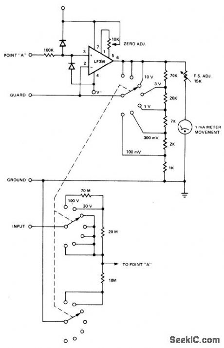
Uses LF356 opamp in noninverting connection to give high input impedance along with diode protection against input overvoltage. On 100-V range, input impedance is 100 megohms. - Signetics, Analog Data Manual, Signetics, Sunnyvale, CA, 1977, p 640-641. (View)
View full Circuit Diagram | Comments | Reading(960)
LOAD_CURRENT_DELAY
Published:2009/7/15 3:01:00 Author:Jessie

Silicon controlled switch circuit delays start of load current for interval of 0.5 RC after switch is thrown.- Transistor Manual, Seventh Edition, General Electric Co. 1964, p 435. (View)
View full Circuit Diagram | Comments | Reading(766)
500_MC_TO_1000_Mc_DOUBLER
Published:2009/7/15 3:01:00 Author:Jessie

Single varactor gives up to 15 w output from 25 w input, with output linear up to 11 w. Conversion efficiency is 50%.-G. Schaffner and J. Cochran, Varactor Diodes and Circuits for High Power Output and linear Response, Motorola Application Note AN-191, Aug.1965. (View)
View full Circuit Diagram | Comments | Reading(699)
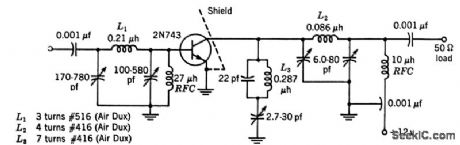
VARACTOR_FREQUENCY_QUADRUPLER
Published:2009/7/15 3:00:00 Author:Jessie

With 50-Mc input, output is 22 w at 200 Mc. Series-tuned idler circuit L3-C4 is omitted for frequency-doubling.-L. E. Clark, E. B. Mack, and R. C. Hejhall, Highlights of Small-Signal Circuit Design, Electronics, 36:49, p 46-50. (View)
View full Circuit Diagram | Comments | Reading(844)
HIGH_IMPEDANCE_DIFFERENTIAL_INPUTS
Published:2009/7/15 3:00:00 Author:Jessie

High impedance for both inputs of differential precision rectifier is provided by two opamps that produce current output for conversion to voltage by instrumentation amplifier A2. Diode bridge in feedback path of opamp A2 provides rectification with precise control for determining voltage drop across R. Design permits accurate measurement of differential AC inputs from millivolts to volts with AC voltmeter.-J. Graeme, Measure Differential AC Signals Easily with Precision Rectifiers, EDN Magazine, Jan. 20, t975, p 45-48. (View)
View full Circuit Diagram | Comments | Reading(1052)
1215_MC_TO_243_MC_DOUBLER
Published:2009/7/15 3:00:00 Author:Jessie

Input is tuned to fundamental and output to second harmonic. Combination series-parallel trap in collector circuit rejects fundamental.-Texas Instruments Inc., Transistor Circuit Design, McGraw-Hill, N.Y., 1963, p 328. (View)
View full Circuit Diagram | Comments | Reading(549)
INTERFACES_FOR_100_OHM_LINE
Published:2009/7/14 4:25:00 Author:May

Permits transferring data signals from SA900/901 diskette storage drive to location of MC6800 microprocessor up to maximum of 20 feet away through 100-ohm coax. Data line drivers used are capable of sinking 100-mA in logic true state with maximum voltage of 0.3 V with respect to logic ground. When line driver is in logic false state, driver transistor is cut off and voltage at output of drive( is at least 3 V with respect to logic ground.- Microprocessor Applications Manual (Motorola Series in Solid-State Electronics), McGraw-Hill, New York, NY, 1975, p 5-211-5-212. (View)
View full Circuit Diagram | Comments | Reading(611)
FLASHTUBE_TRIGGER
Published:2009/7/14 4:25:00 Author:May

Uses 2D21 thyratron switch to discharge capacitor across primary of high-vohage pulse transformer whenever thyratron is fired. Resulting pulse is applied to trigger electrode of flashtube. Fires reliably up to 60 times per second. Used to illuminate number on aluminum indexing wheel on spinning shaft of magnetic gage used to locate exact position of ferromagnetic barrier encapsulated in shaped-charge container.-P. Seward, Magnetic Gage Locates Encased Metal Parts, Electronics, 31:33, p 65-67. (View)
View full Circuit Diagram | Comments | Reading(1776)
TRIPLER_DOUBLER_GIVES_700_1200_MC
Published:2009/7/15 2:59:00 Author:Jessie

First stage is grounded-grid amplifier, with plate tuned by 1-turn coil and variable capacitor. Common-grid tripler and doublet are tuned with coaxial resonators. –A. E. Anderson and H. D. Hern, F-M Exciter For Sight or Scatter Systems,Electronics,31:11, p 148-151. (View)
View full Circuit Diagram | Comments | Reading(804)
8_BIT_PROGRAMMABLE_INPUT
Published:2009/7/14 4:24:00 Author:May

Serves as digitally programmable frequency source covering 10 to 2550 Hz for systems under microprocessor control. Frequency change is essentially instantaneous, assuring immediately valid data. Uses MC1408L8 8-bit monolithic D/A converter to supply constant current for charging C in negative direction. When capacitor voltage exceeds lower negative threshold voltage at pin 3 of LM311 high-impedance comparator A1, comparator changes state and sets 7476 flip-flop.This turns on Q1 through level-shifter Q2, discharging C until it exceeds higher threshold voltage at pin 2 of A2. Flip-flop then resets and C begins charging again. Second half of 7476 serves as divider. To cover above frequency range, values should be: R3.9K; R1 27K; R2 10K; R3 2.2K; C 0.1 μF. Circuit gives 8-bit accuracy. Design equations are presented in article.-A. Helfrick, Eight-Bit Frequency Source Suited for μP Control, EDN Magazine, Sept. 20, 1976, p 116 and118. (View)
View full Circuit Diagram | Comments | Reading(1483)
LOW_NOISE_UHF_PREAMP
Published:2009/7/15 2:59:00 Author:Jessie

Special push-pull input stage using low-noise UHF transistors gives average preamp noise figure as low as 2.2 dB. Can be used with 300-ohm line of broad-band UHF antenna without usual balun trans-former or differential input stage. Balun is used after amplifier to transform push-pull output to input of single-ended second stage without de-grading noise figure. Developed for use with new deep-fringe-area UHF TV antenna having three flat in-line director elements, for over-the-air reception of UHF TV programs in areas previously having no watch able pictures.-J. E. Kluge, Advanced Antenna Design and an Ultra-low-Noise Preamplifier Extend UHF Viewing Area, IEEE Transactions on Broadcasting, March 1977, p 17-22.
(View)
View full Circuit Diagram | Comments | Reading(2276)
SYNCHRONOUS_SAWTOOTH_FOR_PDM_TELE_METRY
Published:2009/7/14 4:24:00 Author:May

Circuit generates highly linear ramp that is reset to zero by each clock pulse. When ramp exceeds analog value of unknown input voltage, pulse is terminated. R1, R2, and C1 form integrating network around opamp. Varying R2 changes slope of ramp output. -J. Springer, Build a Sawtooth Generator with Three ICs, EDN Magazine, Nov. 15, 1970, p 49. (View)
View full Circuit Diagram | Comments | Reading(715)
BLOCKING_OSCILLATOR_SUPPLY
Published:2009/7/14 4:24:00 Author:May
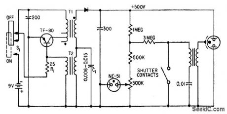
Uses modified blocking oscillator to obtain square wave switching at 4,200 cps. Charges 300-mfd capacitor to 500 v in 5 to 10 sec from 9-v dry cell that can deliver up to 700 Bashes. To start oscillator, S1 momentarily connects R1 to negative side of battery.-H. A. Manoogian, Transistor Photoflash Power Converters, Electronics, 31:35, p 29-31. (View)
View full Circuit Diagram | Comments | Reading(1008)
TUNED_VOLTMETER
Published:2009/7/15 2:58:00 Author:Jessie

Optical Electronics active filter (3704 up to 5 kHz, 3705 up to 50 kHz, or 3706 up to 500 kHz) provides proper scale factor, impedance buffering, and isolation for measuring AC voltages at specific frequency. Circuit provides 100K input impedance and up to 10mA drive for 10-V meter. IC provides independent gain (scale factor or sensitivity), tuning, and Q (selectivity) adjustments.- Tuned Voltmeter, Optical Electronics, Tucson, AZ, Application Tip 10248. (View)
View full Circuit Diagram | Comments | Reading(1067)
PHOTOFLASH_SUPPLY
Published:2009/7/14 4:23:00 Author:May

Flybcck or ringing choke oscillator is free-running when voltage on regulator capacitor C2 is less than zener voltage for reference diode D2, but converter action is halted when desired output voltage is reached. Circuit then periodically replaces charge lost by capacitor leakage.Energy conversion efficiency can therefore exceed 50% theoretical upper limit of most conventional photoflash circuits.-R. J. Sherin, Efficient Photoflash Power Converter, Electronics, 33:4, p 57. (View)
View full Circuit Diagram | Comments | Reading(1275)
_5_V_TO__15_V
Published:2009/7/14 4:32:00 Author:May

Use of switching regulator for voltage conversion permits generation of higher output voltage along with polarity reversal. LM311 operates as free-running MVBR with low duty cycle. Frequency is determined by C1 and R5 and duty cycle by divider R3-R4. Extra loop function performed by Q1 and zener operating in conjunction with resistor network modifies oscillator duty cycle until desired out-put level is obtained. Nominal frequency is 6 kHz, duty cycle is 20% for -15 V output, and maximum load current is 200 mA. Design equations are given.-H, Mortensen, IC Comparator Converts +5 to -15V DC, EDN Magazine, Dec. 20, 1973, p 78-79. (View)
View full Circuit Diagram | Comments | Reading(769)
SINGLE_STAGE_AUDIO_AMPLIFIER
Published:2009/7/15 2:57:00 Author:Jessie

Design procedure is given for basic transistor stage.- Transistor Manual, Seventh Edition, General Electric Co., 1964, p 241. (View)
View full Circuit Diagram | Comments | Reading(1057)
DECADE_DRIVER_FOR_FREQUENCY_MULTIPLIER_
Published:2009/7/15 2:57:00 Author:Jessie
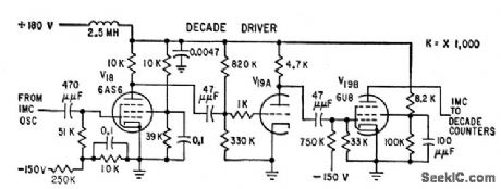
Input signal from frequency-multiplying oscillator is stepped up to 80 v peak-to-peak, with 1-microsec rise time, for accurate triggering of decade counter.-W. O. Brooks, Stepping up Frequency with Counter Circuits, Electronics, 32:29, p 60-62. (View)
View full Circuit Diagram | Comments | Reading(655)
| Pages:629/2234 At 20621622623624625626627628629630631632633634635636637638639640Under 20 |
Circuit Categories
power supply circuit
Amplifier Circuit
Basic Circuit
LED and Light Circuit
Sensor Circuit
Signal Processing
Electrical Equipment Circuit
Control Circuit
Remote Control Circuit
A/D-D/A Converter Circuit
Audio Circuit
Measuring and Test Circuit
Communication Circuit
Computer-Related Circuit
555 Circuit
Automotive Circuit
Repairing Circuit