
Circuit Diagram
Index 637
SOUND_SUBSYSTEM
Published:2009/7/15 4:32:00 Author:Jessie

RCA CA3134 combines sound IF and audio output stages in single IC for use in TV receivers. Input is taken from sound IF output of receiver. Provides electronic volume control with improved taper. Alternate circuit shown provides unattenuated audio output.- Linear Integrated Circuits and MOS/ FETTs, RCA Solid State Division, Somenrville, NJ, 1977, p 368. (View)
View full Circuit Diagram | Comments | Reading(1051)
1_Hz_TO_1_MHz_ADJUSTABLE_WIDTH
Published:2009/7/15 4:31:00 Author:Jessie
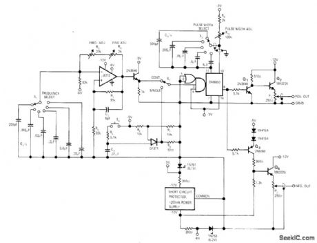
Frequency and pulse width are selected independently in decade steps with rotary switches. Vemier controls provide fine tuning and allow f up to 20% overlap of ranges. Rise and fall times are 100 ns or better. Both positive and negative outputs are provided, each adjustable from 0 to 10 V. S2 gives choice of continuous or single-pulse operation, and pushbutton S4 provides single-pulse outputs. μA710 comparator connected as astable MVBR provides trigger inputs for DM8850 retriggerable mono. Article gives circuit details and design equations.-C. Brogado, Versatile Inexpensive Pulse Generator, EDN|EEE Magazine, Oct. 1,1971, p 37-38. (View)
View full Circuit Diagram | Comments | Reading(752)
ACTIVE_ADJUSTABLE_BANDPASS_AUDIO_FILTER
Published:2009/7/14 3:49:00 Author:May


Has Butterworth attenuation characteristics and 42 db/octave cutoff slopes. Output is 50 v rms with low distortion, and dynamic range over 100 db. Second-order harmonic distortion is reduced by operating tube heaters at low voltage. Seven elements are varied simultaneously by switching different resistor and capacitor values to change cutoff frequencies. Article has three tables giving these values for high-pass cutoffs from 16 to 16,200 cps and low- pass cutoffs from 20 to 20,000 cps.-J. R. MacDonald, Active Bandpass Filter has Sharp Cutoff, Electronics, 31:33, p 84-87. (View)
View full Circuit Diagram | Comments | Reading(1748)
TWO_QUADRANT_SQUARING
Published:2009/7/14 3:49:00 Author:May
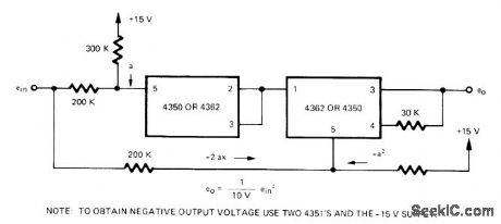
Teledyne Philbrick log modules are used in simple two-quadrant squarer in which input is offset becausemodules accept only one polarity Circuit shown provides positive output voltage.-''Aρplications for Models 4350/4351 & 4362/4363 Logarithmic Amplifiers,″ Teledyne Phillbrick,Dedham,MA ,974, AN-14. (View)
View full Circuit Diagram | Comments | Reading(455)
CRO_AS_TV_MONITOR
Published:2009/7/15 4:31:00 Author:Jessie

Permits monitoring transmitted amateur televison I signals with oscilloscope for such applications as checking sync levels and sync-pulse shape Outgoing signal can be monitored while adjusting modulator -Circuits、73 Magazine, March 1977 p 152. (View)
View full Circuit Diagram | Comments | Reading(840)
SINGLE_FET_CASCODE
Published:2009/7/14 3:49:00 Author:May


Costs less than two-fet version, but has somewhat poorer stability. Voltage gain is 500 for 33,000-ohm output impedance.-B,Smith, Low-Noise FETs sound Good to Circuit signers,Electronics,37:31,p 58-62. (View)
View full Circuit Diagram | Comments | Reading(570)
BIT_RATE_GENERATOR
Published:2009/7/15 4:30:00 Author:Jessie
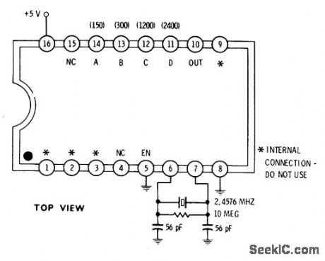
Fairchild 4702 IC synthesizes frequencies most often used in serial data communication, particularly with UARTS. With connections shown, output is 1760 Hz which is 16 x 110-baud rate of serial teletypes. Grounding only pin A generates 16 x 150 bauds. Grounding only pin B gives 16 x 300 bauds, grounding pin C gives 16 x 1200 bauds, and grounding pin D gives 16 x 2400 bauds. Will drive one regular TTL load at supply drain of 1 mA.-D. Lancaster, CMOS Cookbook, Howard W. Sams, Indianapolis, IN, 1977, p 155. (View)
View full Circuit Diagram | Comments | Reading(869)
1_kW_ON_2_METERS
Published:2009/7/14 3:49:00 Author:May

Developed for moonbounce communication. Article covers construction, with emphasis on insulation and cooling, and gives circuit of 3-kV power supply required.-R. W. Campbell, Kilowatt Linear Amplifier for 2 Meters, 73 Magazine, Dec. 1973, p 29-35. (View)
View full Circuit Diagram | Comments | Reading(914)
LINE_DRIVER_FOR_LED
Published:2009/7/15 4:24:00 Author:Jessie

Single-ended input is converted to balanced differential drive for feeding 75-ohm transmission line terminated by LED serving as input for optically coupled line receiver. Logic 1 input is inverted to logic 0 by inverter A, turning on a, and turning off out-put of gate B. At same time, output of inverter A is logic 1, which inhibits turn-on of Q1 and makes output of inverter D go low. Thus, logic 1 input means that current is sourced into line and LED by Q1 then sunk by output of D. Similarly, logic 0 input results in current being sourced into line by Q2 and sunk by inverter B, making diode D1 conduct and turn off LED of OCI receiver. -K. Erickson, Line Driver Is Compatible with OCI Line Receiver, EDN Magazine, Oct. 5, 1976, p 106. (View)
View full Circuit Diagram | Comments | Reading(794)
05_mA_FOR_0_50_KILOHMS
Published:2009/7/14 3:48:00 Author:May
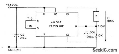
Current source uses Fairchild μA723 voltage regulator operating from ordinary unregulated supply not over 40 VDC. Regulator has built-in 7.15-V reference. Output current is well within 1% of 0.5 mA for load impedances from 0-50k. -L. Nickel, Constant Current Sources, 73 Magazine, March 1974, p29
(View)
View full Circuit Diagram | Comments | Reading(431)
150_W_SWITCH_MODE
Published:2009/7/14 3:47:00 Author:May

Unregulated DC voltage is applied to power Darlington Q1 serving as switch that chops voltage so rectangular waveform is applied to RLC output filter. Average voltage to filter depends on duty cycle of switch. 555 timer operates in mono MVBR mode as pulse generator and pulse-duration modulator. R24 applies varying voltage to pin 5 to modulate pulse duration linearly with respect to applied voltage, Actions of O1, Q2, and Q6 maintain constant 3.6 V at arm of control pot. Q4 and Q5 provide 20-kHz clock pulse, above audible range. Overcurrent protection of transistors is provided by R11, SCR, and Q3. Adjust R11 so SCR turns on and shuts down circuit when current through R11 reaches 8 A. Circuit must be reset manually after overload. Q7 and R10 load circuit to prevent oscillation at low output volt-age and light load.-R. J. Walker, A 150 Watt Switch-Mode Regulator, CQ, March 1977, p 40-43 and 74-75. (View)
View full Circuit Diagram | Comments | Reading(947)
1_MHz_SQUARE_WAVE_FOR_TDR
Published:2009/7/15 4:22:00 Author:Jessie
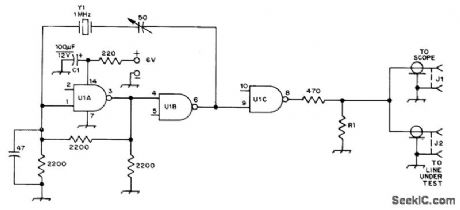
Fast-rise-time 1-MHz pulse generator serves with wide-band CRO and T connector for time-domain reflectometry (TDR) setup used to pinpoint exact location of fault in transmission line. Will also locate multiple faults along line, measure SWR, and measure characteristic impedance of cable. With 1-MHz square-wave source having 500-ns duration for positive portions of wave, cables up to 150 feet long can be tested. R1 should equal characteristic impedance of line being tested. U1 is Signetics N7400A or equivalent quad NAND/NOR gate. Article gives instructions for use.-W. Jochem, An Inexpensive Time-Domain Reflectometer, QST, March 1973, p 19-21. (View)
View full Circuit Diagram | Comments | Reading(2874)
PRECISION_RECTIFIER
Published:2009/7/15 4:22:00 Author:Jessie


Used in digital voltmeters to convert AC waveform to full-waverectified DC equivalent. First 3130 opamp is used as polarity separator, with negative-going signals appearing across upper 10K resistor and positive-going signals across lower 10K resistor. Output of opamp exceeds these voltage drops by exactly diode voltage drop. Second opamp stage recombines positive and negative peaks. 5K trimming pot is adjusted so both peaks are equal height. Output of second opamp is negative-going full-wave replica of input signal. After filtering, output is average DC value in range from 0 to -1.5 V for 0-3 V P-P input.-D. Lancaster, CMOS Cookbook, Howard VV. Sams, Indianapolis, IN, 1977, p 345-346. (View)
View full Circuit Diagram | Comments | Reading(1644)
ASYMMETRICAL_PULSE_GENERATOR
Published:2009/7/15 4:20:00 Author:Jessie
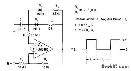
Charge and discharge paths of timing capacitor C1 in LM3900 IC connected as astable oscillator are individually controlled by D1 and D2. Value of R1a controls charge rate of C1 and period t1, while R1b controls discharge rate and period t2. Resistors can be pots for providing variable pulse width and repetition rate. For constant frequency with variable duty cycle, R1 can be single pot with ends going to D1 and D2 and tap going to output. For values shown, t1 is 1 ms and t2 is 4 ms.-W. G. Jung, IC Op-Amp Cook-book, Howard W. Sams, Indianapolis, IN, 1974, p 505.
(View)
View full Circuit Diagram | Comments | Reading(896)
SCR_DRIVER
Published:2009/7/15 4:19:00 Author:Jessie

Two types of blocking oscillators generate required turn-on and turn-off pulses for power-switching output stage of inverter.-R. J. Kearns and J. J. Rolfe, Three .Phase Static Inverters Power Space-Vehicle Equipment, Electronics, 34:18, p 70-73. (View)
View full Circuit Diagram | Comments | Reading(1156)
BUS_TRANSCEIVER
Published:2009/7/15 4:17:00 Author:Jessie

Designed for use in bus-organized data transmission systems interconnected by terminated 120-ohm lines. Up to 27 driver/receiver pairs can be connected to common bus. One two-input NOR gate is included in National DS8641 quad unified bus transceiver package to disable all drivers in package simultaneously.- Interface Integrated Circuits, National Semiconductor, Santa Clara,CA, 1975, p3-17-3-18. (View)
View full Circuit Diagram | Comments | Reading(724)
DUAL_LINE_RECEIVER_FOR_COAX
Published:2009/7/15 4:15:00 Author:Jessie

Single Texas Instruments SN75152 IC contains two receiver sections, each taking input from separate coax. Other receiver section (not shown) is identical and provides similar TTL output for its coax. Driver shown has OR capability for feeding single coax, Receiver has adjustable noise immunity and continuously adjustable hysteresis control (not shown).- The Linear and Interface Circuits Data Book for Design Engineers, Texas Instruments, Dallas, TX, 1973, p 8-78. (View)
View full Circuit Diagram | Comments | Reading(1092)
FOUR_STATE_AMPLIFIER
Published:2009/7/14 3:54:00 Author:May

HA-2400 four-channel programmable amplifier is used with tapped voltage divider in feedback loop to give gains of 1, 2, 4, and 8 controlled by logic inputs to D0 and D1 as shown in truth table. Amplifier is noninverting.-W. G. Jung, IC Op-Amp Cookbook, Howard W. Sams, Indianapolis, IN, 1974, p 431-432. (View)
View full Circuit Diagram | Comments | Reading(660)
PULSE_COUNTER
Published:2009/7/14 3:53:00 Author:May

Unijunction transistor Q1 servos as counter, with other counter stages being identical. Q3 and Q4 energize and lock readout circuit until quench pulse is applied after next counting cycle.-F. W. Kear, Unijuncfion Transistor Pulse-Circuit Design, Electronics, 35:21, p 58-60. (View)
View full Circuit Diagram | Comments | Reading(866)
_12_V_AND__15_V_FROM_4_24_V
Published:2009/7/14 3:53:00 Author:May

Connections shown for Fairchild μA78S40 switching regulator give universal regulator providing either step-up or step-down, for loads up to 100 mA. Efficiency is about 50% for input extremes of 4 and 24 V, increasing to maximum of 75% for other input voltages. Output ripple is essentially eliminated at 12-V output.-R. J. Apfel and D. B. Jones, Universal Switching Regulator Diversifies Power Subsystem Applications, Computer Design, March 1978, p 103-112. (View)
View full Circuit Diagram | Comments | Reading(430)
| Pages:637/2234 At 20621622623624625626627628629630631632633634635636637638639640Under 20 |
Circuit Categories
power supply circuit
Amplifier Circuit
Basic Circuit
LED and Light Circuit
Sensor Circuit
Signal Processing
Electrical Equipment Circuit
Control Circuit
Remote Control Circuit
A/D-D/A Converter Circuit
Audio Circuit
Measuring and Test Circuit
Communication Circuit
Computer-Related Circuit
555 Circuit
Automotive Circuit
Repairing Circuit