
Circuit Diagram
Index 639
ACTIVE_BUTTERWORTH_R_C_FILTER
Published:2009/7/14 3:56:00 Author:May

Article gives design procedure for selecting R and C values for active filters characterized by zero output either at zero frequency or at in infinite frequency. Symmetry of network transfer function allows choice of values by coefficient matching technique. Fifth-order low-pass filter, down 50 db at 70 cps, is shown.-R. E. Bach, Jr., Selecting R-C Values for Active Filters, Electronics, 33:20, p 82-85. (View)
View full Circuit Diagram | Comments | Reading(709)
PROGRAMMED_0_255_V
Published:2009/7/14 3:56:00 Author:May

Uses D/A converter and 2.5-V zener to form digitally programmed voltage reference. Binary-coded TTL information selects voltage ranges of 0-2.55 V or 0-25.5 V. Can be used as lab source having 10 mV per step in low range and 100 mV per step in high range. Output is adjusted with 8-bit input control. R3 determines basic voltage range, being set at 1280 ohms for low range and 12.8K for high range, Although 741 or other general-purpose opamp is adequate for low range, higher-voltage single-supply opamp such as 759 is better for high range and for both ranges, because it gives higher output current on low range.-W. Jung, An IC Op Amp Update, Ham Radio, March 1978, p 62-69. (View)
View full Circuit Diagram | Comments | Reading(639)
UNIJUNCIION_RING_COUNTER
Published:2009/7/14 3:56:00 Author:May

Provides switching for readout and control applications, including data display for airborne digital instrumentation. Q5-Q6 provide resetting.-F. W. Kear, Digital Control Uses Unijunction Transistors, Electronics, 34:18, p 79-80 (View)
View full Circuit Diagram | Comments | Reading(702)
ELECTRONIC_FADER
Published:2009/7/14 3:55:00 Author:May

used to fade audio signals on and off without Producing audible switching transients. signals from matching network of driver are applied to Point A and B.-E. de Boer Electronic Fader for Auditory Research,Electronics,33:50,p 85-87. (View)
View full Circuit Diagram | Comments | Reading(669)
10_MHz_DUAL_CHANNEL_LOGAMP
Published:2009/7/14 3:55:00 Author:May
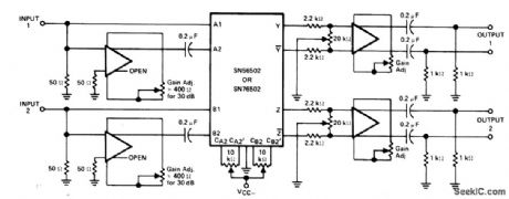
Circuitusing Texas Instruments SN56502 or SN76502 in combination,with four SN52741 oρamps、will handle 50-dB input range perchannel at all frequecies uρ to10 MHz suitable for data compression, analog computation, radar and infrared detection systems, and weapons systems. Differential output voltage levels are generally less than 0.6 V. Output swing and slope of output response are adjusted by varying gain in each channel. Coordinate origin is adjusted with offset pots of output buffers.- The Linear and Interface Circu its Data Book for Design Engineers, Texas Instruments, Dallas, TX, 1973, p 7-46. (View)
View full Circuit Diagram | Comments | Reading(893)
HIGH_VOLTAGENE_GATIVE_SWIT_CHING
Published:2009/7/14 3:55:00 Author:May

Designed for operation from supply voltages above maximum of -40 V for LM304 regulator, Output is -5 V at up to 10 A. Q2 provides volt-age isolation between regulator and Unitrode PIC636 hybrid power switch. R9 limits current through zener under steady-state and start-up conditions.- Switching Regulator Design Guide, Unitrode, Watertown, MA, 1974, U-68A, p 9. (View)
View full Circuit Diagram | Comments | Reading(630)
RING_COUNTER_USES_GATE_TURNOFFS
Published:2009/7/14 3:54:00 Author:May
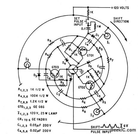
Closing of set pulse input switch turns on first gto. Applying voltage to its lam load. Each shift pulse input then transfers conduction to next gto and lamp.-D.R. Grafham. Now the Gate Turnoff Switch Speeds up D-C Switching Electronics.37:12,p64-71 (View)
View full Circuit Diagram | Comments | Reading(917)
DRIVER_FOR_FADIRA
Published:2009/7/14 3:54:00 Author:May
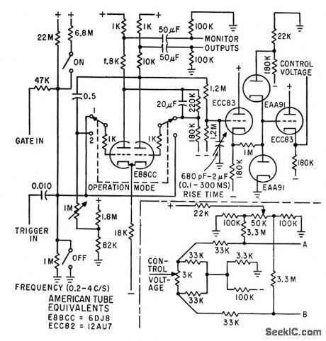
can be operated either in free-funning mode or in triggered orgated mode to produce Control voltage that will drive electronic fader. Correction network at lower right transfers control voltage to fader and minimizes switchingtransient.-E .de Boer, Electronics, Fader for Auditory Research,Electronics, 33:50,p 85-87. (View)
View full Circuit Diagram | Comments | Reading(848)
THYRATRON_AFC_FOR_AIRBORNE_RADAR_1
Published:2009/7/15 4:10:00 Author:Jessie

Uses Foster-Seeley discriminator to produce aeries of pulses varying from zero at crossover to maximum of 0.5 to 2 v at frequency of maximum response. Polarity may be either positive or negative, depending on whether incoming signal is above or below crossover frequency, and can be changed by reversing the diodes. Two thyratrons generate required control voltage for repeller of klystron.-NBS, Handbook Preferred Circuits Navy Aeronautical Electronic Equipment, Vol. 1, Electron Tube Circuits, 1963, p N 13-4. (View)
View full Circuit Diagram | Comments | Reading(1262)
DIFFERENTIAL_LINE_DRIVER
Published:2009/7/15 4:09:00 Author:Jessie

Uses Motorola MC75110L line driver and MC75107L receiver with twisted-pair transmission line having attenuation of 1.6 dB per 100 feet at 10MHz. Clock rate is 18.5 MHz. With push-pull driver shown, single pulse corresponds to transmission of 1 followed by series of 0s; one line is then at ground and the other at -300 mV. Arrangement is suitable for party-line or bus applications. -T. Hopkins, Line Driver and Receiver Considerations, Motorola, Phoenix, AZ, 1978, AN-708A, p 11. (View)
View full Circuit Diagram | Comments | Reading(1088)
HALL_MULTIPLIER_FOR_ANALOG_RATIO_COMPUTER
Published:2009/7/15 4:08:00 Author:Jessie

Indium arsenide Hall plate serves as analog multiplier in circuit with photoresistor R and 2N174 grounded-emitter power amplifier that controls drive current of Hall generator. Differential amplifier A in feedback loop including lamp I controls Hall current. -H. H. Wieder, Analog Ratio Computer Uses Hall Multiplier, Electronics, 36:45, p 46-47. (View)
View full Circuit Diagram | Comments | Reading(1188)
SMOOTHED_D_C_FROM_F_M
Published:2009/7/15 4:08:00 Author:Jessie

Mean d-c level, derived from f-m data on magnetic tape, undergoes R-C smoothing in three-transistor pulse-counting demodulator circuit so output can be fed to cro.-K.R. Whittington, Simple F-M Demodulator for Audio Frequencies, Electronics, 35:48, p89. (View)
View full Circuit Diagram | Comments | Reading(1509)
POLARITY_NONREVERSING_DRIVE
Published:2009/7/15 4:07:00 Author:Jessie

Packard HCPL-2602 optically coupled line receiver handles high data rates from shielded, twisted-pair, or coax cable fed by 745140 line driver, Reflections due to active termination do not affect performance. Peaking capacitor C and series resistor R can be added to achieve highest possible data rate. C should be as large as possible without preventing regulator in line receiver from turning off during negative excursions of input signal. Highest data rates are achieved by equalizing tPLH(propagation delay time to low output level) and tPHL (propagation delay time to high output level).- Optoelectronics Designer's Catalog 1977, Hewlett-Packard, Palo Alto, CA, 1977, p 158-159. (View)
View full Circuit Diagram | Comments | Reading(591)
CRYSTAL_DISCRIMINATOR_IN_AFC_LOOP
Published:2009/7/15 4:07:00 Author:Jessie

Gives narrow bandwidth at 23-Mc crystal frequency, for controlling drift of voltage controlled controlled oscillator.-F. L. Carroll, How to Achieve Stability in Space Telemetry, Electronics, 37:4, p 32-35. (View)
View full Circuit Diagram | Comments | Reading(677)
SQUARE_ROOT_OF_SUM_OF_SQUARES_OF_THREE_VARIABLES
Published:2009/7/15 4:06:00 Author:Jessie

Output signal of Hall-effect squaring multiplier HG is fed to differential amplifier A. Amplified difference controls current through lamp that determines resistance of photoresistor r which, with 2N174, controls Hall current derived from voltage source.-H. H. Wieder, Square-Root Computer Uses Hall Multiplier, Electronics, 37:4, p 30-31. (View)
View full Circuit Diagram | Comments | Reading(847)
BOXCAR_ENVELOPE_DETECTOR
Published:2009/7/15 4:06:00 Author:Jessie

Gives accurate recovery of one-polarity modulation envelope by approximating envelope in level steps between successive peaks of wavetrain. -J. L. Markwalter. Boxcar Envelope Detector,EEE,12:9,p62-63. (View)
View full Circuit Diagram | Comments | Reading(789)
DIODE_PHANTASTRON_AFC_FOR_AIRBORNE_RADAR_1
Published:2009/7/15 4:05:00 Author:Jessie


Pentode is astable phontastron during search and d-c amplifier during lock-on. Operation is nearly independent of tube characteristics. Provides tight control of local oscillator frequency because during lock-on, pentode furnishes direct control of klystron repeller.-NBS, Handbook Preferred Circuits Navy Aeronautical Electronic Equipment, Vol. 1, Electron tube Circuits, 1963, p N 13-6. (View)
View full Circuit Diagram | Comments | Reading(691)
ANALOG_VOLTAGE_MULTIPLIER
Published:2009/7/15 4:05:00 Author:Jessie

Pulse-width modulator and push-pull rectangular pulse generator driving diode-bridge switch give product of two input voltages X and Y, which must be in range of -10 V to +10 V. Input circuit of pulse-width modulator D1-V1 is supplied by 10-kc negative-slope sawtooth and input variable X.-J. Ash and Y. J. Fokkinga, Inexpensive Multiplier for Analog Computers, Electronics, 35:18, p 37. (View)
View full Circuit Diagram | Comments | Reading(1375)
FSK_DETECTOR
Published:2009/7/15 4:04:00 Author:Jessie
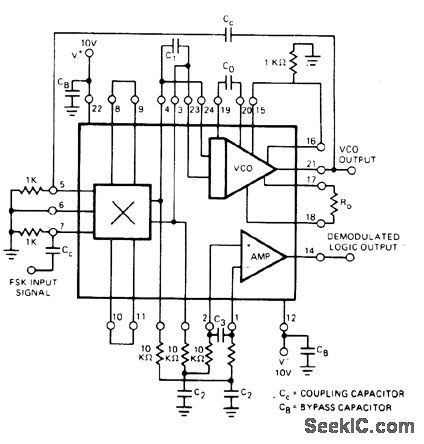
Exar XR-5200 PLL IC is connected as modem suitable for Bell 103 or 202 data sets operating at data transmission rates up to 1800 bauds. Input frequency shift corresponding to data bit reverses polarity of DC out-put voltage of multiplier. DC level is changed to binary output pulse by gain block connected as voltage comparator. - Phase-Locked Loop Data Book, Exar Integrated Systems, Sunny-vale, CA, 1978, p 9-16. (View)
View full Circuit Diagram | Comments | Reading(1172)
EIGHT_CHANNEL_COMPUTERIZED_3SUP1_SUP__SUB2_SUB_DIGIT_VM
Published:2009/7/15 4:04:00 Author:Jessie

Displays up to eight different DC voltages on CRT terminal of microprocessor under key-board control, using BASIC commands and BASIC routine given in article. Uses Motorola MC14433 modified dual-lamp integrating analog-to-digital converter. Unknown voltage is applied to integrator having defined integration time constant for predetermined time limit, to give output voltage proportional to unknown voltage. Computer program substitutes -2,000 V reference from IC2, and circuit keeps track of time for integrator output to move back toward zero. Changing reference to 0.200 V makes same 1999 count represent 199.9 mV full scale. IC1 performs about 25 conversions per second. IC3 and IC4 are output buffers, IC5 is 7474 used as set-reset flip-flop. IC6 is eight-input CMOS multiplexer input.-S. Ciarcia, Try an 8 Channel DVM Cocktail!, BYTE, Dec. 1977, p 76, 78, 80, 92, 94, 96, and 98-103. (View)
View full Circuit Diagram | Comments | Reading(1931)
| Pages:639/2234 At 20621622623624625626627628629630631632633634635636637638639640Under 20 |
Circuit Categories
power supply circuit
Amplifier Circuit
Basic Circuit
LED and Light Circuit
Sensor Circuit
Signal Processing
Electrical Equipment Circuit
Control Circuit
Remote Control Circuit
A/D-D/A Converter Circuit
Audio Circuit
Measuring and Test Circuit
Communication Circuit
Computer-Related Circuit
555 Circuit
Automotive Circuit
Repairing Circuit