
Circuit Diagram
Index 624
PULSE_STRETCHER
Published:2009/7/15 3:15:00 Author:Jessie

Circuit also serves as analog one-shot memory and as peak sense-and-hold with automatic reset. Digital output is logic 0 until CT and RT have decayed by onetime constant, when it goes to logic 1. Pulse duration is RCTC. Analog output amplitude is equal to input amplitude, and duration is same as digital pulse. Optical Electronics 9053 comparator automatically resets circuit after timing interval unless reset is performed manually. Analog output can be used as pulse stretcher with known and controllable pulse duration.- Analog 'One-Shot'-Pulse Stretcher, Optical Electronics, Tucson, AZ, Application Tip 10292. (View)
View full Circuit Diagram | Comments | Reading(3579)
EXPON_ENTIAL_VCO
Published:2009/7/14 4:58:00 Author:May

Can be driven with linear time base of voltage and used with logarithmic frequency display, as in frequency-response tests Useful range of circuit is four decades Values shown give timing-current range of 10 nA to 100 μA, yielding frequency range of 1 Hz to 10 kHz. Input voltage range of 60 mV per decade is obtained from voltage divider R1-R2 to allow higher and more practical value for actual input voltage to circuit. –W. G. Jung, IC Timer Cookbook, Howard W. Sams, Indianapolis, IN, 1977, p 174-179. (View)
View full Circuit Diagram | Comments | Reading(1033)
DYNAMIC_RANGE_COMPRESSOR
Published:2009/7/15 3:15:00 Author:Jessie

Transistorized version of vacuum-lube drawdown limiter or compressor amplifier limits dynamic range of any negative input signal without a threshold or saturation level. Output is approximately proportional to cube root of input, thus giving effective dynamic range compression. Good over audio range, yet can operate up to megacycle region if used with suitable high-frequency transistors and series inductance to varistor. Maximum input signal of 200 my produces 3 v output, corresponding to gain of 15 at maximum permissible compression.-D. E. Lancaster, Dynamic Range Compressor, EEE, 11:2, p 25. (View)
View full Circuit Diagram | Comments | Reading(2320)
SYMMETRY_CORRECTION
Published:2009/7/14 4:58:00 Author:May

Low-cost external correction circuit for MC3420 switching-mode regulator ensures balanced operation of power transformer in push-pull inverter configuration. Circuit senses voltage impressed on primary of T1 through sensing secondary S2, for integration by opamp A1 so voltage on C represents volt-second product applied to T1. During conduction period of Q1, voltage on C ramps up to some positive value and output of A2 is low. Conduction period for output 2 then begins, Q2 turns on, and C ramps down to 0 V. A2 output then goes high, inhibiting output 2 and Q2. Times for Q2 to charge and discharge are equal so conduction periods are equal-H. Wurzburg, A Symmetry Correcting Circuit for Use with the MC3420, Motorola, Phoenix, AZ, 1977, EB-66. (View)
View full Circuit Diagram | Comments | Reading(695)
THEREMIN_VOLUME_CONTROL_CIRCUIT
Published:2009/7/14 4:58:00 Author:May

The circuit shows a capacitive potential divider with volume trim on the fixed oscillator. The hand capacitance loads down the RF to a detector stage, reducing the detector output. This output is used to control the gain of an audio amplifier. (View)
View full Circuit Diagram | Comments | Reading(1818)
HALL_MULTIPLIER_FIELD_COIL_DRIVE
Published:2009/7/15 3:15:00 Author:Jessie

Feedback amplifier drives field coil current in phase with input signal over range of 0 cps to 7 kc, with less than 1.5% distortion. –R. A. Greiner, Feedback Amplification Improves Hall-Effect Multipliers, Electronics, 34:34, p 52-55. (View)
View full Circuit Diagram | Comments | Reading(737)
COSINE_SINE_GENERATOR
Published:2009/7/15 3:14:00 Author:Jessie

Based on fact that area under sine curve varies as cosine function. Input voltage is converted into pulse width that controls electronic switch to cut off one portion of sine wave. Resulting rectangular pulses are symmetrical with respect to positive peak of sine wave.-H. Schmid, Function Generator for Sines or Cosines, Electronics, 32:4, p 48-50. (View)
View full Circuit Diagram | Comments | Reading(737)
0_10_kHz_WITH_0_10_V_CONTROL
Published:2009/7/14 4:58:00 Author:May

CA3130 MVBR generates pulses of constant amplitude V and width T2. Average output voltage is applied to noninverting input of comparator (through integrating network R3-C2. Comparator output signal from pin 6 is fed through R4 and D4 to inverting terminal 2 of A1 for adjusting MVBR interval T3 so EAVG is equal to control voltage.- Linear Integrated Circuits and M0Sf/FET's, RCA Solid State Division. Somerville, NJ, 1977, p 269.
(View)
View full Circuit Diagram | Comments | Reading(662)
EXPONENTIAL_FUNCTION_GENERATOR
Published:2009/7/15 3:14:00 Author:Jessie

Output is exponentially decoying curve in which exponent is determined by other components of system. Used in analog computer to integrate curve of dye concentration in blood stream to obtain now role.-R. L. Skinner and D. K. Gehmlich, Analog Computer Aids Heart Ailment Diagnosis, Electronics, 32:40, p 56-59. (View)
View full Circuit Diagram | Comments | Reading(901)
POLARITY_REVERSING_DRIVE
Published:2009/7/14 4:57:00 Author:May

Half of 9614 polarity-reversing line driver feeds Hewlett-Packard HCPL-2602 optically coupled line receiver through shielded、twisted-pair、or coax cable. Data rate is improved considerably by using Schottky diode at input of receiver. Best data rates are achieved when tPHL (propagation delay time to low output level) and tPLH (propagation delay time to high output level) are closest to being equal,- Optoelectronics Designer's Catalog 1977, Hewlett-Packard, Palo Alto, GA, 1977、p 158-159. (View)
View full Circuit Diagram | Comments | Reading(695)
28_V_AT_100_W
Published:2009/7/14 4:56:00 Author:May

Circuit using Delco DTS-1020 Darlington silicon power transistor operates over input range of 22-28 V. Switching rate is 9 kHz. Efficiency is about 85% at full load. Out-put voltage is sensed to control pulse width of mono MVBR which is triggered at 9 kHz by os-cillator.- 28 Volt Darlington Switching Regulator, Delco, Kokomo, IN, 1971, Application Note 49, p 4. (View)
View full Circuit Diagram | Comments | Reading(639)
THEREMIN
Published:2009/7/14 4:56:00 Author:May

The theremin uses several RF oscillators connected to antennas to both generate audio frequencies and vary the volume of the note produced. The pitch is generated by heterodyning two oscillators, one fixed and one variable, and the volume is controlled by another pair of oscillators in which the beat frequency that is generated is used to derive a control voltage for the volume-control circuit. (View)
View full Circuit Diagram | Comments | Reading(0)
1_kHz_VCO
Published:2009/7/14 4:56:00 Author:May

Changes in control voltage input are used to vary nominal 1-kHz output of CD4007 CMOS voltage-controlled oscillator proportionately. Values of R and C can be changed to obtain other nominal frequencies.-W. J. Prudhomme, CM0S Oscillators, 73 Magazine, July 1977, p 60-63.
(View)
View full Circuit Diagram | Comments | Reading(2378)
REZEROING_AMPLIFIER
Published:2009/7/14 4:55:00 Author:May
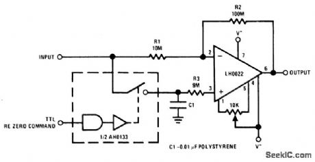
Used where input signal has unknown and variable DG offset, as in telemetry applications. Rezero command line is enabled while ground reference signal is applied to input, making C1 charge to level proportional to DC offset of system. When rezero line is deactivated, amplifier becomes conventional inverter, subtracting system offset and giving true ground-referenced output. For 10-V full-scale system requiring 0.1% (10-mV) accuracy, amplifier needs rezeroing reference every 100 ms.- Linear Applications, Vol. 1, National Semiconductor, Santa Clara, CA, 1973, AN-63, p 1-12. (View)
View full Circuit Diagram | Comments | Reading(619)
_5_V_SWITCHING
Published:2009/7/14 4:54:00 Author:May

Unitrode U2T201 Darlington serves as switching element for LM304 step-down switching regulator operating from input of -25 V. Operating frequency can be about 25 kHz. Darlington will handle peak currents up to 10 A.- Designer's Guide to Power Darlingtons as Switching Devices, Unitrode, Watertown, MA, 1975, U-70, p 10. (View)
View full Circuit Diagram | Comments | Reading(804)
TELEPHONE_QUALITY_CODER_DECODER
Published:2009/7/14 4:54:00 Author:May
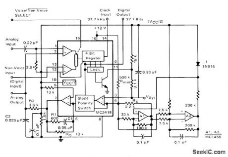
Uses Motorola MC3418 continuously variable slope delta modulator-demodulator IC to give over 50 dB of dynamic range for 1-kHz test at 37.7K bit rate. At this rate, 40 voice channels can be multiplexed on standard 1.544-megabit telephone carrier facility. IC includes active companding control and double integration for improved performance in encoding and decoding digital speech. Opamp types are not critical.- Continuously Variable Slope Delta Modulator/ Demodulator, Motorola, Phoenix, AZ, 1978, DS 9488. (View)
View full Circuit Diagram | Comments | Reading(1254)
VACUUM_TUBE_THEREMIN_VOLUME_CONTROL_CIRCUIT
Published:2009/7/14 4:53:00 Author:May

Gain is controlled by a variable negative grid bias in an audio amplifier stage. This oscillator produces a negative dc voltage by means of a rectifier. As a hand is brought up to the volume plate antenna, this loads the oscillator, reducing output and hence the negative dc output. This means increased gain for the controlled audio stage. (View)
View full Circuit Diagram | Comments | Reading(981)
THEREMIN_CIRCUIT_VOLUME_SECTION
Published:2009/7/14 5:08:00 Author:May

The player's hand capacitance loads down the RF to a detector stage, reducing the detector output. This output is used to control the gain of an audio amplifier in the pitch section. (View)
View full Circuit Diagram | Comments | Reading(892)
DIGITAL_RECORDING_WITH_CASSETTES
Published:2009/7/14 5:08:00 Author:May

Circuit shows modifications required for standard cassette recorder to bring read level up to about 1 V. Recorder works well over range of 100 to 1200 b/s. During write process, direct current is passed through record head to saturate tape, with polarity depending on direction of current. During read cycle, voltage is induced in head winding only when transition between oppositely polarized zones moves past head. 555 timer is used as combination level detector and flip-flop to recover serial data.-R. W Burhans, A simpler Digital Cassette Tape Interface, BYTF, Oct 1978, p 142-143. (View)
View full Circuit Diagram | Comments | Reading(845)
D_C_SUPPLY_FOR_FLUOURESCENT_LAMPS
Published:2009/7/14 5:06:00 Author:May

Lamp operates directly from d-c supply, without a-c conversion. Transistors form constant-current source that controls lamp current. Q3 is controlled by Schmitt trigger Q1.Q2. When lamp current exceeds preset value, voltage drop across 5.6-ohm resistor turns on Q1, thereby turning off Q2 and Q3. When lamp current falls, Q3 comes on again. To start, pushbutton closes circuit through lamp heaters and shunts 5.6-ohm resistor to give faster heating. When button is released, voltage surge caused by series inductor ignites lamp. Control circuit then varies lamp current 25% above and below its average value at 1-kc rate. Regulator losses are only 3 w.-D. B. Hoisington, Direct Current Regulator Drives Fluorescent Lamps, Electronics, 39:17, p 94-95. (View)
View full Circuit Diagram | Comments | Reading(878)
| Pages:624/2234 At 20621622623624625626627628629630631632633634635636637638639640Under 20 |
Circuit Categories
power supply circuit
Amplifier Circuit
Basic Circuit
LED and Light Circuit
Sensor Circuit
Signal Processing
Electrical Equipment Circuit
Control Circuit
Remote Control Circuit
A/D-D/A Converter Circuit
Audio Circuit
Measuring and Test Circuit
Communication Circuit
Computer-Related Circuit
555 Circuit
Automotive Circuit
Repairing Circuit