
Circuit Diagram
Index 630
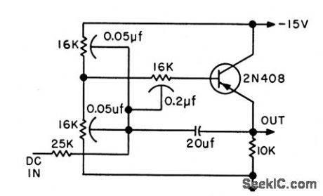
RANDOM_FLASH_GENERATOR
Published:2009/7/14 4:32:00 Author:May

Multivibrators generate single pulse to drive flash tube at unspecified time of from 2 to 10 seconds after switch is closed.-P. Scott, Microflash and Pulse Stimulator Tests Human Response, Electronics, 34:27, p 48-51. (View)
View full Circuit Diagram | Comments | Reading(621)
SIMPLE_DOUBLER
Published:2009/7/15 2:57:00 Author:Jessie
Uses distributed R.C networks consisting of resistive and conductive layers on dielectric substrate, with d-c applied between electrodes at 65 v for doubling frequency of ceramic-dielectric 400-cps oscillator.-M. M. Perugini, Race to Reduce Capacitor Size, EEE, 10:7, p 61-64. (View)
View full Circuit Diagram | Comments | Reading(719)
LASER_MODULATOR_CURRENT_CONTROL
Published:2009/7/14 4:31:00 Author:May

When modulator or pumping current for laser is lost, output voltage of pulse transformer T1 will rise to limit set by zener D12, which then conducts lo make Q2 and Q3 absorb current not required by energy storage capacitors.-S.J. Grabowski Pulse Power Supply Design for Laser Pumping Electronics,36:51,p33-35. (View)
View full Circuit Diagram | Comments | Reading(735)
25_MHz_VIDEO_PREAMP
Published:2009/7/15 2:56:00 Author:Jessie
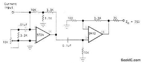
Uses Optical Electronics 9724 opamp for input stage and 9412 opamp for output stage. Current input can be from vidicon or image orthicon camera tube. Input compensation can be adjusted to provide aperture correction. Feedback network for input opamp minimizes effects of stray capacitance Values shown give 1-V output for 1-μA input.-“A 25 MHz Video Preamplifier-Line Drivel,” Optical Electronics, Tucson, AZ, Application Tip 10195. (View)
View full Circuit Diagram | Comments | Reading(910)
UNDERWATER_CAMERA_FLASH
Published:2009/7/14 4:31:00 Author:May

Film drive motor and camera shutter are interlocked with electronic flash so camera can be operated blindly at depths up to 6 miles, with lash occurring only when shutter is open.. Adjustable mechanical time-delay switch S1 delays start of operating cycle until camera is at operating depth. Timing switch S2 then takes picture every 12 sec for two hours.-H. E. Edgerton and S. O. Raymond, Instrumentation for Exploring the Oceans, Electronics, 33:15, p 62-63. (View)
View full Circuit Diagram | Comments | Reading(900)
LINEAR_READOUT_CIRCUIT
Published:2009/7/14 4:30:00 Author:May


Thermistors have found their way into a number of temperature-sensing applications. However, their resistance is a nonlinear function of temperature. In many applications, a digital readout of the thermistor also is desired. It is possible to produce a digital signal with a frequency that is linearly proportional to the temperature. The entire active portion of the circuitry can be implemented using 3/4 of an LM339. Comparator A is configured to operate as an op amp that generates voltage (Vt) which is inversely proportional to the thermistor's resistance, Rt. The voltage Vt is used as the thresh-old for the relation oscillator formed by comparators B and C. Comparator B monitors the voltage on the integrating capacitor (Vc). When it crosses Vt, it triggers the one-shot formed by comparator C via the signal Vtrig The output of comparator C resets the integrating capacitor for a duration, to, where to= (R2+3 kΩ)C2. Then the cycle begins again. The circuit achieves linear readout because the exponential nonlinearity of the thermistor is compensated by the exponential decay of the voltage in the relaxation oscillator. (View)
View full Circuit Diagram | Comments | Reading(985)
50_150_MC_TRIPLER
Published:2009/7/15 2:56:00 Author:Jessie

Charge-storage 1N4386 varactor triples frequency with power efficiency of 70% for input of 50 watts.-G. Schaffner, Charge Storage Vcractors Boost Harmonic Power, Electronics, 37:20, p 42-47. (View)
View full Circuit Diagram | Comments | Reading(797)
RECEIVE_FILTER
Published:2009/7/14 4:30:00 Author:May

Used as prefilter having controlled group-delay distortion, ahead of receiving modem in data transmission system. Values shown are for 950-1400 Hz answer filter. For 1900-2350 Hz originate filter, change critical values to those given in parentheses. -D. Lancaster, TV Typewriter Cookbook, Howard W. Sams, Indianapolis, IN, 1976, p 180-182. (View)
View full Circuit Diagram | Comments | Reading(787)
FET_OUTPUT_STAGE
Published:2009/7/15 2:56:00 Author:Jessie

Bootstrapped input, Darlington driver, and White follower give voltage gain of one, input impedance of 1 meg, and output impedance of 10 ohms.-B. Smifh, Low-Noise FETs Sound Good To Circuit Designers, Electronics, 37:31, p 58-62. (View)
View full Circuit Diagram | Comments | Reading(1076)
SCR_CONTROLS_PHOTOFLASH
Published:2009/7/14 4:29:00 Author:May

C1 is charged to 100 v by ac power supply. Input trigger pulse fires 2N1597 scr to make C1 discharge through primary of T1. Peak of 5 kv in secondary triggers photoflash. Maximum repetition rate is 20 flashes per second.-E. L. Harris, Jr., Solid ,State Components Shrink Photoflash Control, Electronics, 36:15, p 70. (View)
View full Circuit Diagram | Comments | Reading(608)
OPTICALLY_COUPLED_DATA_LINK
Published:2009/7/14 4:28:00 Author:May
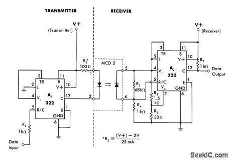
322 comparator at transmitter end of link drives LED of MCD 2 optoisolator which accepts TTL input. Receiver is similar comparator having additional biasing to match photodiode output of Output optoisolator. Complete system is noninverting,with delay of about 2 μs. Receiver can have any supply within 4.5-40 V range of 322. Transmitter should be matched to its supply voltage by selecting R2 according to equation shown.-W. G. Jung, IC Timer Cookbook, Howard VV. Sams, Indianapolis, IN, 1977, p 156-15.
(View)
View full Circuit Diagram | Comments | Reading(1040)
TRANSISTORS_SWITCH_10_AMP_PULSES_FOR_LIGHT_EMITTING
Published:2009/7/14 4:28:00 Author:May

Input A must precede and follow B by 1 microsec to give 1-microsec width for 10-width for 10-amp pulses driving light-emitting diodes at repetition rates up to 100 kc.-E. L. Bonin, Drivers for Optical Diodes, Electronics, 37:22, p 77-82. (View)
View full Circuit Diagram | Comments | Reading(696)
DRIVER_FOR_UGHT_DIODE
Published:2009/7/14 4:26:00 Author:May


When blocking oscillator is triggered, its output controls flashes from light-emitting diode. Triple-winding transformer gives maximum output for minimum power-supply drain.-C. H. Moulton, Light Pulse System Shrinks High-Voltage Protection Device, Electronics, 38:11, p 71-75. (View)
View full Circuit Diagram | Comments | Reading(704)
50_DUTY_CYCLE
Published:2009/7/14 4:26:00 Author:May


Provides 80 flashes per minute. Scr's conduct alternately in parallel inverter with capacitor commutation, and are triggered by free-running relaxation oscillator Q1. Flashing rate is determined by R1-R2-C1.-D. V. Jones, Quick-On-The-Trigger Design, Electronics, 38:12, p 105-110. (View)
View full Circuit Diagram | Comments | Reading(694)
LOCKED_90°OUTPUTS
Published:2009/7/14 4:26:00 Author:May

Delivers two-phase (sine and cosine) outputs locked together. Frequency can be varied over wide range by altering bias current with 10K pot that produces common-mode output voltage in NE5596 multiplier IC driving 8038 ICs serving as VC0s. Triangular outputs of oscillators are fed to multiplier inputs for phase control. Lower-cost 566 VCO can be used if sinusoidal outputs are not needed. Phase error over tuning range is nominally zero, whereas with conventional phase locked loop circuitry the capture range may be exceeded or phase error can be large.-J. M. Worley, Two-Phase V. C.O., Wireless World, Dee. 1976, p 41.
(View)
View full Circuit Diagram | Comments | Reading(1007)
WAVEFORM_EDGE_PULSER
Published:2009/7/15 3:34:00 Author:Jessie

Circuit generates square-wave output pulse for each edge of square-wave input. EXCLUSIVE-OR gate is used as programmable inverter that returns point C to quiescent low state following each transfer of data through 5474 IC. When used for frequency-doubling, input waveform should be symmetrical because output is proportional to propagation delay of flip-flop plus delay of 5486 EXCLUSIVE-OR gate.-D. Giboney, Double-Edge Pulser Uses Few Parts, EDN Magazine, Dec. 15, 1972, p 41. (View)
View full Circuit Diagram | Comments | Reading(811)
EMITIER_CURRENT_CONTROL_40_MC_AFC_OSCILLATOR
Published:2009/7/15 3:34:00 Author:Jessie

Error signal, usually derived from external discriminator, is applied in series with base bias network to give sensitivity of about 1.5 Mc per v and nearly straight voltage-frequency characteristic.-T. P. Prouty, Using Varactors to Extend Frequency-Control Range, Electronics,36:45, p 48-49. (View)
View full Circuit Diagram | Comments | Reading(657)
LINEAR_AMPLIFIER
Published:2009/7/15 3:33:00 Author:Jessie

Motorola MHW-710 power module boosts 1-W output of VHF Engineering TX-432B crystal-controlled solidstate exciter to about 10 W for simple amateur TV transmitter. Interconnections are made with short lengths of FIG-174 coax. Input jack J1 is connected to exciter by 50 ft of RG-174, and length is gradually reduced until proper drive level is obtained for linear operation. RFC uses 8 turns No. 22 enamel on 1-megohm 1-W resistor. To cover 400-440 MHz, use MHW-710-1; for 440-470 MHz, use MHW-710-2.-R. E. Taggart, Interested in Television?, 73 Magazine, Oct. 1977, p 164-174. (View)
View full Circuit Diagram | Comments | Reading(2370)
24_V_D_C_TO_SQUARE_WAVE_A_C
Published:2009/7/15 3:33:00 Author:Jessie

Will replace sine-wave source because square wave output is modified by series saturable reactor to have same rms and average values as pure sine wave.-D. Levy, Replacing Sine Wave Sources with Solid-Stale Inverters, Electronics, 34:26, p 80-83. (View)
View full Circuit Diagram | Comments | Reading(1069)
POWER_SWITCH_FOR_SWITCHING_REGULA_TOR
Published:2009/7/14 4:23:00 Author:May

Circuit operating from 12-V step-down transformer includes push-pull driver providing interface between logic drive signal and 2N6306 high-voltage power transistor. Switching is provided at 3 A and 20 kHz, with artificial negative bias supply created from single positive supply to improve fall time. Current limiting is added to base current to limit overdrive and reduce storage time. Power switch is turned off by forcing IC to logic low. Used in 24-V 3-A switching-mode power supply operating from AC line.- R. J. Haver, A New Approach to Switching Regulators, Motorola, Phoenix, AZ, 1975, AN-719,p5. (View)
View full Circuit Diagram | Comments | Reading(703)
| Pages:630/2234 At 20621622623624625626627628629630631632633634635636637638639640Under 20 |
Circuit Categories
power supply circuit
Amplifier Circuit
Basic Circuit
LED and Light Circuit
Sensor Circuit
Signal Processing
Electrical Equipment Circuit
Control Circuit
Remote Control Circuit
A/D-D/A Converter Circuit
Audio Circuit
Measuring and Test Circuit
Communication Circuit
Computer-Related Circuit
555 Circuit
Automotive Circuit
Repairing Circuit