
Circuit Diagram
Index 634
METER_AMPLIFIER
Published:2009/7/15 4:48:00 Author:Jessie
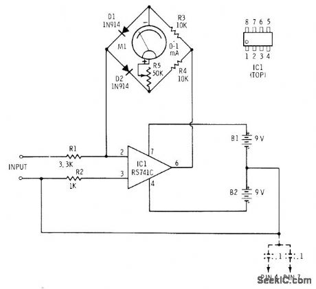
Meter in feedback path of opamp is connected in bridge circuit for measuring both AC and DC voltages. Input voltage is equal to meter current in amperes multiplied by 3 times value of R1 in ohms; with 3.3K and 0.1 mA, input is 0.99 V. Multiplying milliampere reading of meter by 10,000thusgives input voltage. If long supply leads cause oscillation, connect 0.1-μF capacitors between ground and supply pins 4 and 7 as shown.-F. M. Mims, Integrated Circuit Projects, Vol. 4, Radio Shack, Fort Worth, TX, 1977, 2nd Ed., p 54-60. (View)
View full Circuit Diagram | Comments | Reading(0)
TRIPLE_TUNED_90_OHM_INPUT
Published:2009/7/14 4:10:00 Author:May

Article gives design procedure. Example shown passes signals between 55 and 65.5 Mc.-R. B.Hirsch, How to Design Bandpass Triples, Electronics, 32:34, p 41-44. (View)
View full Circuit Diagram | Comments | Reading(656)
FET_VOLTMETER
Published:2009/7/15 4:47:00 Author:Jessie

With FET in one leg of Wheatstone bridge, meter has input impedance of over 1 megohm. With no input voltage, adjust R4 so meter reads zero. With 9-V battery, RI can be adjusted for full-scale meter reading of 8 V. With 12-V battery, meter range is 0-10 V.-F. M. Mims, Transistor Projects, Vol. 2, Radio Shack, Fort Worth, TX, 1974, p 59-66. (View)
View full Circuit Diagram | Comments | Reading(0)
PROGBAMMED__DIVIDE_BY_179
Published:2009/7/14 4:09:00 Author:May

Produces symmetrical output waveforms even if divider ratios are large, variable, and even or odd. Circuit is set up for output of N = 179, for which M= 89 is programmed into divider and odd/even control of logic is a .0 Control logic can be simplified, depending on particular requirements; thus, if perfect symmetry is notessential,G4 and FF4 can be eliminated, Article tells how to program for any other value of N.-V. R. Godbole, Programmable Divider Maintains Output Symmetry, EDN Magazine, July 5, 1974, p 72-74.
(View)
View full Circuit Diagram | Comments | Reading(639)
VOLTAGE_CONTROL
Published:2009/7/14 4:09:00 Author:May

Improved voltage-con-trolled current source uses complementary transistors in opamp feedback loop. Common-mode voltage at input to opamp is always near zero. Circuit was designed for use in integrator having ground-referenced integrating capacitor, to produce 1 mA/V. R3a and R3b sense current through Q1 and Q2 so voltage proportional to difference is fed back to input of opamp for comparison with input voltage. Zener voltages determine quiescent-current level. Frequency response is limited to 1 MHz by performance of specified opamp.-P. T. Skelly, Voltage-Con-trolled Current Source, EDN/EEE Magazine, Aug. 1, 1971, p 45-46. (View)
View full Circuit Diagram | Comments | Reading(1754)
16_30_MHz_20_W_LINEAR_DRIVER
Published:2009/7/14 4:09:00 Author:May

Broadband amplifier using inexpensive plastic RF power transistors provides total power gain of about 25 dB for driving SSB transmitter power amplifiers to levels up to several hundred watts. Supply is 13.6 V. Circuit is stable even with load mismatches of 10:1.-H. 0. Granberg, Low-Distortion 1.6 to 30 MHz SSB Driver Designs, Motorola, Phoenix, AZ, 1977, AN-779, p 3.
(View)
View full Circuit Diagram | Comments | Reading(717)
VARIABLE_BANDWIDTH_848_KC_CRYSIAL_FILTER
Published:2009/7/14 4:09:00 Author:May

High-Q unbalanced crystal filter is easy to adjust over appreciable frequency range,Can be used in f-m oscillators, signal generators, and i-f amplifiers, as well as in variable-bandwidth filters.-J. C. Seddon, Stable Crystal Filter is Parallel Resonant, Electronics, 31:11, p 155-156. (View)
View full Circuit Diagram | Comments | Reading(680)
FLIP_FLIP_RING_COUNTER
Published:2009/7/14 4:09:00 Author:May

Complementary mvbr, in which Q1 and Q2 are either both on or both off, gives low power drain. Strong negative pulse applied to base of Q2 of first stage gives reset.-J. E. Russell, Ten Signals at a Glance, Electronics, 37:19, p 54-57. (View)
View full Circuit Diagram | Comments | Reading(724)
100_MEG_INPUT_RESISTANCE
Published:2009/7/14 4:08:00 Author:May
High d-c input resistance is obtained with grounded-collector circuit operating under starved conditions. A-c input impedances of 100 megare obtain-able at audio frequencies, as required for photoconductive devices.-B. M.Bramson, Starved Transistors Raise D-C Input Resistance, Electronics, 32:5, p 54-55. (View)
View full Circuit Diagram | Comments | Reading(912)
BANDPASS_ANSWER_FILTER
Published:2009/7/15 4:47:00 Author:Jessie

Provides gain of 15 dB over bandwidth of 1020 to 1320 Hz for low-speed modem system using Motorola MC6860 IC. Attenuation is 35 dB at 2225 Hz, as required for answer-only modem system. Equations for values of filter components are given.-J. M. DeLaune, Low-Speed Modem System Design Using the MC6860, Motorola, Phoenix, AZ, 1975, AN-747, p 10. (View)
View full Circuit Diagram | Comments | Reading(565)
800_CPS_OSCILLATOR_WITH_PARALLEL_T_FILTER
Published:2009/7/14 4:08:00 Author:May

R-C network in feedback loop determimes frequency of oscillation.-T. Mollinga, Active parallel-T Networks, EEE, 14:4, p 93-98. (View)
View full Circuit Diagram | Comments | Reading(687)
MONO_PULSE_SHRINKER
Published:2009/7/15 4:45:00 Author:Jessie

Duty cycle of clock pulse is shortened by two CMOS inverters used to form negative-transition triggered mono-stable multivibrator. Duration of output pulse T is about 1.4R1C1. Output pulse occurs each time input clock goes from high to low. Used with foldback current limiting for short-circuit protection in clock-driven regulated power supply. Low duty cycle of dock pulses ensures positive full-load starting of supply.-J. L. Bohan, Clocking Scheme Improves Power Supply Short-Circuit Protection, EDN Magazine, March 5, 1974, p 49-52. (View)
View full Circuit Diagram | Comments | Reading(1249)
TWISTED_PAIR___TERMINATIONS
Published:2009/7/15 4:44:00 Author:Jessie

National DS7830 line driver applies digital data to twisted-Pair transmission line in high-noise environment, and DS7820 line receiver responds to data signals at other end of line while providing immunity to noise spikes. Exact value of C1 depends on line length. Supply voltage is 4.5 to 5 V for both receiver and driver, C2 is optional and controls response time. - Interface Integrated Circuits, National Semiconductor, Santa Clara, CA, 1975, p8-1-8-16. (View)
View full Circuit Diagram | Comments | Reading(1467)
GAIN_PROGRAMMED_AMPLIFIER
Published:2009/7/14 4:08:00 Author:May
8-bit multiplying D/A converter using cascaded 4-bit sections provides logic-controlled gain for signal preconditioning, level control, and dynamic range expansion. Logic 0 turns JFET switch on, and logic 1 turns switch off. Series FET in feed-back path of opamp compensates for ON resistance of JFET switch. Circuit has gain of 0.9996 (binary) with 5K feedback resistor and gain of 0.99 (BDC) with 8K feedback resistor.- FET Databook, National Semiconductor, Santa Clara, CA, 1977, p 6-47-6-49. (View)
View full Circuit Diagram | Comments | Reading(1095)
20_KC_RING_COUNTER
Published:2009/7/14 4:07:00 Author:May

Shift pulses turns off conducting sillicon controlled switch by reverse-biasing cathode gate. Charge stored on coupling capacitor then triggers next gate.- Transistor Manual, Seventh Edition, General Electric Co. 1964, p 431. (View)
View full Circuit Diagram | Comments | Reading(827)
HIGH_SPEED_PULSES
Published:2009/7/15 4:44:00 Author:Jessie

TTL circuit provides dual-polarity microsecond pulses. Pulse amplitude is adjusted by changing zeners D1, D2, or R3. Design overcomes slew-rate problems associated with most opamps.-L. Johnson, Dual-Polarity Pulses from TTL Logic, EDN Magazine, April 20, 1974, p 91.
(View)
View full Circuit Diagram | Comments | Reading(672)
_12_V_AND__15_V_FROM_5_V
Published:2009/7/14 4:07:00 Author:May

Uses Fairchild μA78S40 switching regulator having variety of internal functions that can provide differing voltage step-up, step-down, and inverter modes by appropriately connecting external components. External NPN transistor Q3 boosts step-up regulator, and NPN transistor Q4 increases series-pass regulator output well above 1 A. Total of 1.5 A is available from two outputs. Transistor and diode types are not critical. Efficiency is 80% for 15-V output and 64% for :2-V output.-R. J. Apfel and D. B. Jones, Universal Switching Regulator Diversifies Power Subsystem Applications, Computer Design, March 1978, p 103-112. (View)
View full Circuit Diagram | Comments | Reading(539)
PLL_FOR_001_Hz_TO_100_kHz
Published:2009/7/15 4:43:00 Author:Jessie

Highly stable and precise phase-locked loop system using Exar XR-2207 VCO and XR-2208 operational multiplier is suitable for wide range of applications in data transmission and signal conditioning. Supply voltage range is 16 V to ±13 V. For 10-kHz center frequency, Rois 10K and Co is 0.01μF. R1 and C1 which determine tracking range and low-pass filter characteristics, are 45K and 0.032μF,- Phase-Locked Loop Data Book, Exar Integrated Systems, Sunnyvale, CA, 1978, p 62-64. (View)
View full Circuit Diagram | Comments | Reading(945)
2_STAGE_R_C_COUPLED_AUDIO_AMPLIFIER
Published:2009/7/14 4:07:00 Author:May

Input impedance for basic circuit is about 1300 hms. Design equations are given.- Transistor Manual, Seventh Edition, General lectric Co., 1964, p 242. (View)
View full Circuit Diagram | Comments | Reading(2233)
Q_MULTIPLIER_FOR_F_M_MONITOR
Published:2009/7/15 4:43:00 Author:Jessie

Checks calibration of f-m and television transmitter percentage-of-modulation monitors by using Q multiplier with monitor to make Bessel function measurements.-D. S. Henry, Cali-brating Broadcost Modulation Meters, Electronics, 33;16, p 67. (View)
View full Circuit Diagram | Comments | Reading(1562)
| Pages:634/2234 At 20621622623624625626627628629630631632633634635636637638639640Under 20 |
Circuit Categories
power supply circuit
Amplifier Circuit
Basic Circuit
LED and Light Circuit
Sensor Circuit
Signal Processing
Electrical Equipment Circuit
Control Circuit
Remote Control Circuit
A/D-D/A Converter Circuit
Audio Circuit
Measuring and Test Circuit
Communication Circuit
Computer-Related Circuit
555 Circuit
Automotive Circuit
Repairing Circuit