Circuit Diagram
Index 623
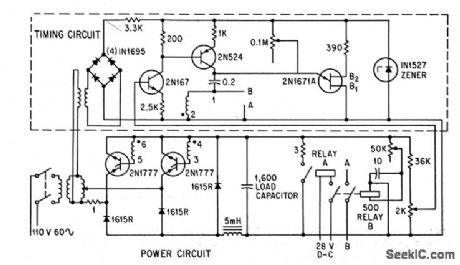
CONSTANI_CURRENT_CAPACITOR_CHARGER
Published:2009/7/14 5:08:00 Author:May

Firing angle of a-c supply voltage is decreased in steps after each supply cycle, to match charging rate of 360-mfd capacitor for 30-kw plasma pinch space engine. So current pulses have identical average peak of 8.6 amp.-F. Ellern. Capacitance Chargers for Space Employ Controlled Rectifiers, Electronics.36:41,p32-33 (View)
View full Circuit Diagram | Comments | Reading(813)
O_to_2440_MICROSEC_BOOTSTRAP_DELAY
Published:2009/7/15 3:28:00 Author:Jessie

Is triggered by gating mvbr. Receives control voltage from ten-turn potentiometer calibrated in distance units. Output drives blocking oscillator through transformer. Accuracy is about 1% of delay setting.-NBS, Hand-book Preferred Circuits Navy Aeronautical Electronic Equipment, Vol. 1, Electron Tube Circuits, 1963, p N9-2. (View)
View full Circuit Diagram | Comments | Reading(546)
TEMPERATURE_COMPENSATED_CONSTANT_CURRENT_GENERATOR
Published:2009/7/14 5:26:00 Author:May


Reverse voltage characterisitic of zener, in conjunction with baseemitter characteristic of transistor, stabilizes collector current by maintaining constant voltage across R from-55 to+25℃.-Temperature-Compensated constant Current Generator. Electronic Circuit Design Handbook, Mactier Pub.Corp.N.Y.1965,P169. (View)
View full Circuit Diagram | Comments | Reading(644)
PRECISION_CONSIANT_CURRENT_SUPPLY
Published:2009/7/14 5:25:00 Author:May

Reference amplifier, consisting of integrated zener diode and npn transistor, acts with Q2 to maintain constant reference voltage across R4. Current through R4 equals load current except for relatively small base currents of Q2 and Q3. Current drift over l5 hours is less than 0.01%.- Trclnsislor Manual, Seventh Edition, General Electric Co.1964, p 233. (View)
View full Circuit Diagram | Comments | Reading(957)
CD4528_CMOS_TIMER
Published:2009/7/14 5:24:00 Author:May

The CMOS timer shown here can easily be cascaded with other similar 4528 circuits. R1C1 and R2C2 determine the timiing. (View)
View full Circuit Diagram | Comments | Reading(4429)
TRANSISIOR_OVERLOAD_PROTECTION
Published:2009/7/14 5:24:00 Author:May

Current greater than 3 amp flowing through 0.47-ohm resistor in emitter of current-switching transistor Q1 drops voltage on base of Q2, causing Q2, Q3, and Q4 to saturate. Q3 opens circuit immediately and keeps it open for duration of overload, For complete short-circuits, Q4 latches K2 to provide positive protection.-F. W. Kear, Fast-Response Over-loud Protection, Electronics, 33:7, p125. (View)
View full Circuit Diagram | Comments | Reading(654)
CASSETTE_PLAYBACK_OF_CW_AND_RTTY
Published:2009/7/14 5:23:00 Author:May

Playback-signal conditioning circuit is used between tape recorder and transmitter when routine CW calls or RTTY test messages are re-corded on endless-loop cassette recorder. Recorded tone is rectified by :N4148 and applied to RC timing circuit. Decay voltage developed across network when tone is removed turns on 2N3904 and 2N3906 stages. Output of 2N3906 drives reed relay in transmitter keying circuit. if resistor is used in place of relay, drop across it during key-down period can be used to drive electronic keyer,-Cassette-Aided CW and RTTY, 73 Magazine. Sept. 1977, p 122-123. (View)
View full Circuit Diagram | Comments | Reading(620)
CONSTANT_CURRENT_GENERATOR
Published:2009/7/14 5:23:00 Author:May

Provides 28 microamp, regulated within 0.75% over range of -20 to +60℃, to feed emitters low-level differential amplifier. Circuit compensates for base-emitter voltage change with temperature.-M. Wolpert and D. Spooner, Temperature Compensated Constant-Current Generator, EEE, 12:12, p 58. (View)
View full Circuit Diagram | Comments | Reading(839)
FAST_TURN_ON_PLAYBACK_PREAMP
Published:2009/7/14 5:22:00 Author:May

Turn-on for gain and supply voltage is only 0.1 s, as com-pared to 5 s normally required in preamp providing NAB tape playback response.- Audio Handbook, National Semiconductor, Santa Clara, CA, 1977, p 2-31-2-37. (View)
View full Circuit Diagram | Comments | Reading(615)
LONG_PERIOD_TIMER
Published:2009/7/14 5:22:00 Author:May

This circuit is based on the 7240 CMOS programmable timer chip (IC3), which has an accuracy of 0.5 percent. It contains a time-base generator, the frequency of which is decided by a resistor and a capacitor. The basic time period is RC seconds; so, given that the maximum value of R is 10 MΩ and the maximum value of C is 1000μF, the maximum time period is 10,000 seconds, (2.8 hours) IC3 also has an eight-stage binary divider chain. The total period available is 27 times the above, which is just over 14 days. In this figure, S1 is an optional power switch. S2 is the switch which is closed to initiate timing. Closing S2 generates a brief low pulse that goes to pin 11 of the timer IC3 and starts the timing. The output of the timer is normally high, but it goes low for the whole of the timing interval. The length of the interval is selected by a rotary switch S3. Pins 1 to 8 of IC3 are the outputs from the eight-stage divider chain. When the counter is reset, they all go high; while timing, they go through an inverted binary sequence. R5 connects the output to the RESET terminal (pin 10), so the counter is reset at the end of the interval. The first stage of the logic consists of two NOR gates and a NAND gate wired as an inverter (part of IC1, 4011). These gates detect the two alarm states. A high output on either pin 8 or pin 9 causes a low output from gate IC2c (pin 10). This makes the RESET input of IC4 low. IC4 is a 14-stage counter with its own oscillator, which begins to oscillate when the RESET is made low. The oscillator has a period of about 25 kHz, which is divided down to produce 1.6 kHz at pin 7 (high-pitched note), 200 Hz at pin 6 (low-pitched note), 6 Hz at pin 1 (fast bleeping), and 1.5 Hz at pin 3 (slow beeping). The remainder of the logic consists of gates producing the fast high-pitched bleep signal, which goes to the red LED (D1) by way of transistor TR2, and the slower, low-pitched bleep, which goes to the green LED (D2) by way of TR3. Both signals go to the speaker LS1 by way of TR1. (View)
View full Circuit Diagram | Comments | Reading(0)
50000_AMP_SINGLE_PULSE_CURRENT_SWITCH_
Published:2009/7/14 5:21:00 Author:May

Simple triggered-gap switch operates at voltage down to 1kv to control switching with time jitter of only 0.1 microsec between successive pulses. Can be used for magnetron testing, surge-current generator, and flash-lamp source. Output of trigger generator is clomped sine wave having sufficient amplitude to break down gap in switch and initiate current pulse. V1 and V2 serve as sharpener for triggering pulse.-E. H. Cullington, W. G. Chace, and R.L. Morgan. Low-Voltage Trigger Controls High Currents, Electronics, 31:15, p 86-88. (View)
View full Circuit Diagram | Comments | Reading(1063)
CW_AND_RTTY_ON_CASSETTES
Published:2009/7/14 5:21:00 Author:May

Circuit provides conditioning of routine CW calls or PTTY test messages, as required for recording on end-less-loop cassette. Keyed signal is filtered to remove contact bounce, then used to turn on 2N3906 which gates 2N2646 sawtooth oscillator operating at about 5 kHz when using 0.005-μF gate capacitor; for lower frequency, increase capacitor to 0.01μF.-Cassette-Aided CW and RTTY, 73 Magazine, Sept, 1977, p 122-123. (View)
View full Circuit Diagram | Comments | Reading(620)
COPYING_CASSETTE_PROGRAMS
Published:2009/7/14 5:19:00 Author:May

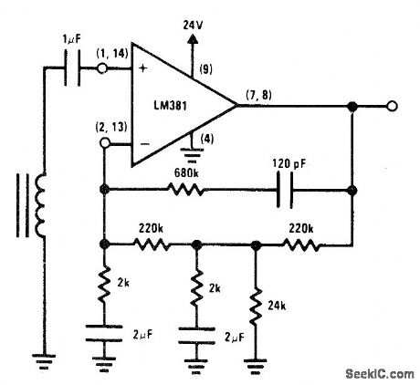
Controller serves for making duplicate copies of microprocessor programs recorded on magnetic tape, for insurance against accidental damage to master cassette during use. Used between audio out- put of cassette player and audio input of tape recorder. Opamp IC1 with gain of 100 overloads so output is constant-amplitude square wave regardless of input level from tape being copied. If program uses audio tones for digital data, eight cycles of 2400 Hz represents digital 1 and four cycles of 1200 Hz represents digital O. Additional opamps act as four-pole Butterworth filter rejecting signals above 3000 Hz. 10K pot is adjusted so output level matches requirements of recorder,-P. A. Stark, Copying Computer Cassettes, Kilobaud, Aug. 1978, p 94-96. (View)
View full Circuit Diagram | Comments | Reading(681)
RANDOM_NOISE_ANALYZER
Published:2009/7/15 3:19:00 Author:Jessie


Provides digital information from which amplitude probability distribution function and probability density function can be plotted. Consists of two amplitude comparators followed by logic circuits and sampling network.-D. Hoffman and E. Schutzman, Statistical Analysis of Noise-Signal Amplitudes, Electronics, 32:30, p 48-49. (View)
View full Circuit Diagram | Comments | Reading(713)
250_W__60_CPSUAL_TRANSFORMER_IN_VERTER
Published:2009/7/15 3:18:00 Author:Jessie

Provides square-wave output to load from 12-v d-c supply, at 130 v, with efficiency of 85%.-Texas Instruments Inc, Transistor Circuit Design, McGraw-Hill, N,Y,J1963,p 458. (View)
View full Circuit Diagram | Comments | Reading(565)
CASSETTE_INTERFACE_1
Published:2009/7/14 5:19:00 Author:May

Used between recorder and computer for loading data stored in tape cassette. Single divider network R1-R2 drives both opamp inputs and provides stabilized sensitivity. R3 isolates inputs.-B. E. Rehm, The TDL System Monitor Board, BYTE, April 1978, p 10, 12-14, and 16. (View)
View full Circuit Diagram | Comments | Reading(555)
COMPOSITE_COLOR_SIGNAL_GENERATOR
Published:2009/7/15 3:18:00 Author:Jessie

Single LM1889 encoder chip produces standard composite color video signal from separate sync.burst flag, 3.579545-MHz subcarrier and 0-4 V red, green, and blue inputs. Subcarrier should be 1-5 V P-P. Modulated RF output can go to cable input of TV set through 75-ohm cable. Applications include TV mixing and video games.-L. Trottier and B. Matic, Signal Encoder Generates Composite Color, EDN Magazine, Aug, 20, 1978, p 148 and 150. (View)
View full Circuit Diagram | Comments | Reading(2593)
TIME_AMPLIFIER
Published:2009/7/15 3:18:00 Author:Jessie

Output pulse width is linear function of input pulse width. With two stages, circuit con amplify nanosec pulse widths to seconds. Article gives design procedure for choosing values of R1, C1, and R2 for desired time amplification and input pulse range. For input of 0.1-1 microsec and time amplification of 1,000, R1 = 51, C1 8,200 mfd, and R2 3.2 meg. For 10-100 microsec input and amplification of 100, R1 is increased to 510 ohms For 100 to 1.000 microsec input and amplification of 10, R1 = 510, C1 = 0.82 mfd, and R2 =320K,-R.W.Fergus, Time Amplifier,EEE,11:8, p 26-27. (View)
View full Circuit Diagram | Comments | Reading(821)
SINE_COSINE_APPROXIMATOR
Published:2009/7/15 3:17:00 Author:Jessie

Converts triangular first approximation of sine and cosine of azimuth angle to accurate approximation of these functions by use of two diode-connected triodes as function generators, one for positive signals and the other for negative signals.-B.L. Bair, Logical Design of SAGE Input Monitor, Electronics,31:33, p 78-81. (View)
View full Circuit Diagram | Comments | Reading(599)
SQUARING_CIRCUIT
Published:2009/7/15 3:16:00 Author:Jessie

Fet gives higher accuracy and higher gain than ordinary transistors or vacuum lubes. At maximum input, output voltage is about three times input voltage. Used to measure mean-squared value of voltages from 5 cps to 100 kc.-Increase the Accuracy of Your Squaring Circuits with Silicon Field-Effect Transistors (Texas Instruments ad), EEE, 11:7, p 6-7. (View)
View full Circuit Diagram | Comments | Reading(658)
| Pages:623/2234 At 20621622623624625626627628629630631632633634635636637638639640Under 20 |
Circuit Categories
power supply circuit
Amplifier Circuit
Basic Circuit
LED and Light Circuit
Sensor Circuit
Signal Processing
Electrical Equipment Circuit
Control Circuit
Remote Control Circuit
A/D-D/A Converter Circuit
Audio Circuit
Measuring and Test Circuit
Communication Circuit
Computer-Related Circuit
555 Circuit
Automotive Circuit
Repairing Circuit