
Circuit Diagram
Index 626
LINEAR_VCO_1
Published:2009/7/14 4:44:00 Author:May

Operates over control-voltage range of +10 mV to +10 V to provide either square or triangle outputs from 5 Hz to 5 kHz, Can be used for instrumentation or electronic music applications.- W. G. Jung, IC Timer Cookbook, Howard W. Sams, Indianapolis, IN, 1977, p 174-179.
(View)
View full Circuit Diagram | Comments | Reading(887)
GAIN_PROGRAMMABLE
Published:2009/7/14 4:41:00 Author:May

Gain of non-inverting opamp can be programmed with standard digital logic levels. With input at 0 V, Q1 is turned on but is held out of saturation by Schottky diode D2. Resulting opamp gain is (R1 + R2)/R2.If R2 is 1.13 kilohms and R1 10 kilohms, gain is 10. When input is 5 V, Q1 is off and gate of Q2 is driven to -15 V. Gain now becomes (R1 + R2 + R3)/(R2 + R3). If R3 is 8.87 kilohms, gain is 2.-K. Karash, Gain-Programmable Amplifier, EEE Magazine, Sept. 1970, p 89. (View)
View full Circuit Diagram | Comments | Reading(884)
FLASH_TIMER
Published:2009/7/14 4:35:00 Author:May

Provides properly synchronized flash illumination for cameras in response to subcarrier pulse commands from uhf receiver.-F. M. Gardner and L. R. Hawn, Camera Control System for Rocket Sled Tests, Electronics, 33:14, p 63-65. (View)
View full Circuit Diagram | Comments | Reading(526)
POLARITY_REVERSING_SPLIT
Published:2009/7/14 4:34:00 Author:May

PHASE DRIVE-Half of 9614 polarity-reversing line driver feeds pair of Hewlett-Packard HCPL-2602 optically coupled line receivers through coax cable. Cable-grounding switches A and B change performance Closing only switch B enhances common-mode rejection but reduces propagation delay slightly. Closing both switches optimizes data rate. Schottky diodes at receiver inputs improve data rate, NAND flip-flop at output greatly improves system noise rejection in split-phase termination of line.- Optoelectronics Designer's Catalog 1977, Hewlett-Packard, Palo Alto,CA,1977,p158-159. (View)
View full Circuit Diagram | Comments | Reading(774)
CONSTANT_CURRENT_REGULATOR
Published:2009/7/14 4:33:00 Author:May

Uses transistor ad variable series resistor. Current will remain within 10% of 10 ma from short circuit up to maximum load of 400 ohms. - Zener Diode Handbook, International Rectifier Corp., 1960, p59. (View)
View full Circuit Diagram | Comments | Reading(992)
FILM_TIMING_MARK_GENERATOR
Published:2009/7/14 4:33:00 Author:May
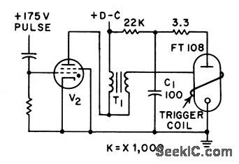
Instrumentation recorder for plasma studies uses discharge of capacitor at beginning of each plasma pinch discharge to trigger lash tube, light from which is chopped by glass disk driven at constant speed by synchronous motor.-J. J. Pearson, Instrumentation for Plasma Propulsion, Electronics, 33:24, p 66-69. (View)
View full Circuit Diagram | Comments | Reading(727)
CURRENT_MODE_SWITCH_FOR_LIGHT_EMITTING_DIOE
Published:2009/7/14 4:33:00 Author:May

Peak currents of 2 amp ,with 50 nsec and fall, drive diode to give pulse-light communication. -E.L. Bonin, Drivers for Optical Diodes, Electronics, 37:32, p 77-82. (View)
View full Circuit Diagram | Comments | Reading(787)
TEMPERATURE_MONITOR
Published:2009/7/14 4:41:00 Author:May

The temperature sensor is a resistor, R4, with negative temperature coefficient (NTC); the resistance of such a resistor drops when its temperature rises. Resistors R4 and R3 are part of a resistance bridge whose variable branch consists of R1, R2, and P1. The metering diagonal is connected to the inputs of comparator IC1a. The voltage at the inverting input of IC1a is set with P1 to a level that with normal temperatures is a little lower than that at the noninverting input. When the temperature rises, the resistance of R4 falls. This results in the comparator's changing state (to low), which causes the piezo buzzer to sound. Care should be taken to ensure that the voltage across the metering diagonal does not drop below 3.5 V to prevent the common-mode dynamic range of the LM393 from being exceeded. The NTC can be a 5- or a 10-kΩ type. It must be in good thermal con-tact with the heat source. Preset P1 must be set to a position where, after the part or device being monitored has attained normal operating temperature, the buzzer just does not sound. The buzzer must be a 5-V type. (View)
View full Circuit Diagram | Comments | Reading(0)
HALLOWEEN_PUMPKIN_BLINKER
Published:2009/7/14 4:40:00 Author:May

Neon lamps blink alternately in eyes of pumpkin for 0.5-sec duration, with 0.5 sec between blinks. Will also serve as roadsid blinker .Although NE2's can be used, LNE17's can be brighter and more effective.-More Glow.Lamp Circuits, EEE, 12:2, p 106-108. (View)
View full Circuit Diagram | Comments | Reading(794)
LINEAR_VCO
Published:2009/7/14 4:40:00 Author:May

Two sections of LM3900 quad linear opamp provide linear response for inputs of 2-12 VDC, Circuit can be adjusted with 1-megohm pot so 4-V input produces 400-Hz square wave at output, 5 V gives 500 Hz, etc. First opamp is connected as integrator and second as Schmitt trigger. When Schmitt output is high, transistor is turned on and diverts current away from noninverting input so integrator output ramps down toward ground.-C. Sondgeroth, More PLL Magic, 73 Magazine, Aug. 1976, p 56-59. (View)
View full Circuit Diagram | Comments | Reading(0)
TWO_LAMP_STROBE_BOOSTS_FLASH_RATE
Published:2009/7/14 4:39:00 Author:May

Two discharge tubes provide shared cycle of operation, to boost stroboscope firing rate to 1,000 flashes per second. tamp circuit, with range-switched discharge capacitors, receives triggers in alternation.-L. H. Barrett, New Circuit Improves Stroboscope Versatility, Electronics, 32:32, p 116-118. (View)
View full Circuit Diagram | Comments | Reading(873)
FLASH_DELAY
Published:2009/7/14 4:39:00 Author:May

Supressor-gated sanatron pentode provides adjustable delay for changing spacing of lashes.-P. Scott, Microflash and Pulse Stimulator Tests Human Optical Response, Electronics, 34:27, p 48-51. (View)
View full Circuit Diagram | Comments | Reading(684)
±15_V_TRACKING
Published:2009/7/14 4:39:00 Author:May

Dual-tracking connection for Fairchild μA78S40 switching regulator operates from single 20-V input Efficiency is 75% for+15 V and 85% for -15 V, both at 100 mA. Output ripple is 30 mV.-R. J. Apfel and D. B. Jones, Universal Switching Regulator Diversifies Power Subsystem Applications, Computer Design, March t978, p 103-112, (View)
View full Circuit Diagram | Comments | Reading(2022)
FLASH_TUBE_DRIVE
Published:2009/7/14 4:39:00 Author:May

Generates low-impedance positive pulses having adjustable amplitude but constant durcttion, for driving flash tube to give same intensity-time characteristic as other fiash tubes having different colors.-P. Scott, Microflash and Pulse Stimulator Tests Human Optical Response, Electronics, 34:27, p 48-51. (View)
View full Circuit Diagram | Comments | Reading(736)
FUNCTION_GENERATOR
Published:2009/7/15 3:13:00 Author:Jessie

Desired function of input voltage is developed across RC and inverted by Q4. One application is for computing ground range of radar target front slant range. Transistors eliminate need for d-c amplifier.-D. R. Chick, Boosting Function Generator Output with Transistors, Electronics, 33:13, p 75-76. (View)
View full Circuit Diagram | Comments | Reading(5388)
BALANCED_LIN_E_TRANSMISSION
Published:2009/7/14 4:38:00 Author:May
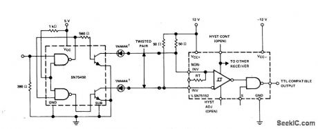
Transmits data at rates up to 0.5 MHz over twisted pair to Texas Instruments SN75152 dual-line receiver. Other section of receiver is identical and can handle additional twisted-pair input. Diodes in lines are required only for negative common-mode protection at driver outputs. System has high common-mode voltage capability. SN75450 is dual peripheral driver for high-current switching at high speeds.- The Linear and Interface Circuits Data Book for Design Engineers, Texas Instruments, Dallas, TX, 1973, p8-78. (View)
View full Circuit Diagram | Comments | Reading(1058)
SQUARE_LAW_OUTPUT
Published:2009/7/15 3:12:00 Author:Jessie

Diode network and detector provide output proportional to square of input voltage. Input range of 40 db is split into two 20-db segments. Each stage saturates and gives constant output for voltages above operating range. For voltages below operating range, stage is cut off and has zero output. Combination of two stages gives desired square-law characterisitic. Resistor values are: R1A, R3A a=3.18K,R1B=57.9K, R3B=18.75K, R5 =3K、R7=10, R2A, R4B =5.06K, R4A =0.86K, R2B =64.2K,R6 = 300 and R8, R9 = 990.-R. J. Matheson, Square-Law Defector has 40-db Dynamic Range, Electronics, 39:18, p 95-97. (View)
View full Circuit Diagram | Comments | Reading(989)
FAST_SYNCHRONIZING
Published:2009/7/14 4:38:00 Author:May

Combination of phase splitter and DAC provides accurate synchronization of high-stability VCO with external reference frequency. IC divides reference frequency by 4 and provides two signals 90° apart, while IC2 divides VC0 frequency similarly by 4. Phase relationship between outputs of IC3 depends on whether VCO is higher or lower than reference, while frequency of IC3 outputs depends on difference between oscillator and reference frequencies, Schmitt triggers IC4 and IC5 supply clock and up/down control to counter IC6. If VC0 frequency is low, IC6 counts up at rate proportional to frequency difference and delivers increasing control voltage to VCO as required for increasing oscillator frequency.-H. W. Cooper, Oscillator Synchronizer Is Fast Acting, EDN Magazine, July 20, 1973, p 83-84. (View)
View full Circuit Diagram | Comments | Reading(1124)
PHOTOELECTRIC__FUNCTION__GENERAIOR
Published:2009/7/15 3:11:00 Author:Jessie

Open-loop photoelectric function generator generates any single-value function With 1%accuracy, as required for duplicating particular antenna patterns in radar simulator. Uses horizontal sweep of 10 millisec (100 cps) with 5-kc vertical sweep.-B. Silverberg, Function Generator for Radar Simulator, Electronics, 32:2, p 52-55. (View)
View full Circuit Diagram | Comments | Reading(678)
STROBE_RATEMETER
Published:2009/7/14 4:38:00 Author:May

Flash role is metered by measuring mean charging current through capacitor supplied With constant-amplitude pulse voltage,-L. H. Barrett, New Circuit Improves Stroboscope Versatility, Electronics ,32:32,p 116-118. (View)
View full Circuit Diagram | Comments | Reading(778)
| Pages:626/2234 At 20621622623624625626627628629630631632633634635636637638639640Under 20 |
Circuit Categories
power supply circuit
Amplifier Circuit
Basic Circuit
LED and Light Circuit
Sensor Circuit
Signal Processing
Electrical Equipment Circuit
Control Circuit
Remote Control Circuit
A/D-D/A Converter Circuit
Audio Circuit
Measuring and Test Circuit
Communication Circuit
Computer-Related Circuit
555 Circuit
Automotive Circuit
Repairing Circuit