
Circuit Diagram
Index 632
TWO_TRANSISTOR_CURRENT_MODE_SWITCH
Published:2009/7/14 4:17:00 Author:May

With two separate voltage supplies, input pulse triggers transistors to give 2-amp pulses for driving light-emitting diode.-F, .Bonin, Drivers for Optical Diodes, Electronics, 37:22, p 77-82. (View)
View full Circuit Diagram | Comments | Reading(790)
120_150_MHz_FOR_TRANSISTOR_RADIO
Published:2009/7/15 5:02:00 Author:Jessie

Values shown cover bands for aircraft radio, 2-m amateur radio band, and other services. Circuit is regenerative converter, with incoming signal tuned by La-C2 and mixed in 2N2222 or equivalent transistor connected as oscillator with frequency controlled by L3 and C7. Difference frequency is adjusted to fall in standard broadcast band, for pickup by radio when converter is mounted close to ferrite loop. For local stations, antenna of converter can be 19-in length of wire. L2 and L4 are 100-μH chokes or about 20 in of fine wire wound on 100K resistor. -S. Kelly, Simple VHF Monitor, 73 Magazine, July 1976, p160. (View)
View full Circuit Diagram | Comments | Reading(2467)
REMOTE_DATA_STATION
Published:2009/7/15 5:00:00 Author:Jessie

Circuit monitors DC voltages applied to pins 19 and 20 of IH5060 multiplexer and converts them to digital format for transmission as serial data to remote microprocessor. IM6100 remote host processor sends control signals to IM6402 UART to select individual multiplexer channels. Single 7209 oscillator provides clock signal for A/D converter and UART. Developed for use with Intercept Jr. microprocessor system.-S. Osgood, Remote Data Station Simplifies Data Gathering, EDN Magazine, Jan. 20, 1978, p 38 and 41. (View)
View full Circuit Diagram | Comments | Reading(874)
HYSTERESIS_AND_DELAY_OSCILLATOR
Published:2009/7/15 4:59:00 Author:Jessie

Separate noninteracting frequency and duty-factor controls permit construction of simple telemetry oscillators having inherently linear transfer function. Absolute synchronization of independent and dependent variables is obtainable with relatively simple pulse-generating circuits. Synchronization cannot be lost. Average value of threshold voltage is maintained constant. Adjustment of hysteresis gap width moves threshold voltage limits symmetrically about average value. Resistance portion of RC delay is switched from positive to negative voltage symmetrically also. Article covers circuit operation in detail.-W. H. Swain, True Digital Synchronizer Employs Hysteresis-and-Delay Element, EDN Magazine, Jan. 1, 1971, p 33-35. (View)
View full Circuit Diagram | Comments | Reading(814)
SWEEP_FOR_SSTV__MONITOR
Published:2009/7/15 4:59:00 Author:Jessie

Uses two 555 timers. one as oscillator and other as linear sawtooth generator,Adjust R4 so oscillator period is slightly longer than interval between sync pulses. When sync is lost. oscillator runs very close to correct frequency and locks in again instantly on first good sync pulse. Circuit also has pulse stretcher, along with lamp driver that operates from horizontal sync pulses for use as tuning indicator,-R,L, Anderson. 555 Timer Sweep Circuit for SSTV 73 Magazine, May1976, p 134-136. (View)
View full Circuit Diagram | Comments | Reading(798)
TRANSISTOR_MAGNETIC_INVERTER
Published:2009/7/15 4:59:00 Author:Jessie

Signal conversion performance is comparable to that of electromechanical vibrator converters. For power conversion, can be substituted for dynamotor in producing high voltage from low-voltage d-c power source.-C. H. R .Campling, Magnetic Inverter Uses Tubes or Transistors, Electronics, 3:11, p 158-161. (View)
View full Circuit Diagram | Comments | Reading(692)
LOW_LEVEL_5_MC_TUNNEL_DIODE
Published:2009/7/14 4:17:00 Author:May
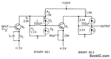
With 1N2933 germanium tunnel diode, power consumption is only 525 microwatts per transistor and binary stage. Circuit voltage and resistances are such that only one tunnel diode is in high-voltage state at a time. Silicon transistors, for coupling, can be pnp or npn.-E. Gottlieb and J. Giorgis, Tunnel-Diode Switching Circuits, Electronics, 36:27, p26-31. (View)
View full Circuit Diagram | Comments | Reading(1014)
PULSED_DEMODULATOR
Published:2009/7/15 4:58:00 Author:Jessie

Used to provide voltage to modulating anode of klystron power amplifier at control totes above 10 cps, in system that controls output power of uhf tropospheric communications links in ac cordance with received signal at opposite end of link, to compensate for fading.-L. P.Yeh, Loop Controls Scatter Power to Offset Fading, Electronics, 32:5, p 60-62. (View)
View full Circuit Diagram | Comments | Reading(584)
LOG_ANTILOG_DIVIDER
Published:2009/7/14 4:16:00 Author:May

Can be used in applications where both numerator and denominator are restricted to single polarity (to onequadrant),Input variables X, Y andZ are applied to three indeρendent transd log amplifiers(A1- Q1A, A2- Q2A, and A3-Q2B ).Outputs of logamps are proportional to logarithms of input variables. R4, in feedback circuit of A4 converts collector current of Q1B to output voltage proportional to VZ VY / VX. Circuit performs multiplication and division simultaneously and with equal accuracy. Overall nonlinearity can be as low as 0.05%. Article gives design equations.-L.Counts and D. Sheingold, Analog Divider:WhatChoice Do You Have?, EDN Magazine, May 5, 1974, p 55-61. (View)
View full Circuit Diagram | Comments | Reading(695)
SYNCHRONOUS_DETECTOR
Published:2009/7/15 4:57:00 Author:Jessie

Linear deteclion permits variation of bandwidth after detection in pcm receivers. Also used us a-m detector and for measuring phase and amplitude of unmodulated signcds.-G. S. Parks, Detector Circuit Measures Phose and Amplitude, Electronics, 38:12, p 84-85. (View)
View full Circuit Diagram | Comments | Reading(1213)
TRANSFORMING__12_V_TO__15_V
Published:2009/7/14 4:16:00 Author:May
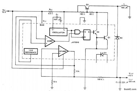
External PNP transistor Q3 and catch diode Q2 (types not critical) are used with Fairchild μA78S40 switching regulator so no pin of IC substrate has voltage more negative than substrate, which is grounded. Efficiency is 84% with 200-mA load. Output voltage ripple is 50 mV but can be reduced by increasing value of C0.-B. J. Apfel and D. B. Jones, Universal Switching Regulator Diversifies Power Subsystem Applications, Computer Design, March 1978, p 103-112. (View)
View full Circuit Diagram | Comments | Reading(877)
ADJUSTABLE_SQUARE_WAVES
Published:2009/7/15 4:57:00 Author:Jessie
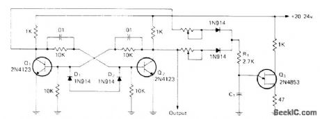
Q1 and Q2 form flip-flop, with UJT Q3 connected as time delay. When power is applied, one flip-flop transistor conducts and C1 charges through one pot and diode. When C1 reaches firing voltage of UJT, it conducts and resulting output pulse triggers flip-flop, Sequence of events now repeats, with C1 charging through other diode. By proper selection of C1 and pot values, circuit becomes square-wave generator with each pot controlling duration of one half-cycle. With one pot replaced by fixed resistor, circuit becomes pulse generator with other pot controlling pulse-repetition rate. If equal-value fixed resistors replace pots and R1 is changed to pot, circuit becomes symmetrical square-wave generator with pot controlling frequency,-I. Math, Math's Notes, CQ, April 1974, p 64-65 and 91-92. (View)
View full Circuit Diagram | Comments | Reading(1000)
TRANSISTOR_AS_SMOOTHING_FILTER
Published:2009/7/14 4:16:00 Author:May

Single junction transistor in liter network of low-voltage power supply permits use of smaller fiber capacitors and chokes. Used in calibrating d-c meters up to 1 amp, at which residual peak-to-peak ripple values are 0.0015 amp and 0.005 v.-F. Oakes and E. W. Lawson, Transistor Filters Ripple, Electronics, 31:15, p 95. (View)
View full Circuit Diagram | Comments | Reading(820)
IMPROVING_TV_SOUND
Published:2009/7/15 4:57:00 Author:Jessie

AF signal from volume control of TV receiver is converted to FM signal by using BC107 transistor to frequency-modulate tunnel-diode oscillator operating within FM broadcast band. Oscillator output is fed through air-core transformer and coaxial line to FM receiver of high-fidelity sound system. Arrangement eliminates most of distortion introduced in power amplifier and loud-speaker of average TV set. Use shielding to keep unwanted FM radiation at minimum.-A. J. Smith, Improving Television Sound, Wireless World, Aug, 1973, p 373. (View)
View full Circuit Diagram | Comments | Reading(2338)
45_30_V_SWITCHING_AT_6_A
Published:2009/7/14 4:14:00 Author:May

LM105 positive regulator serves as amplifier-reference for LM195 power transistor IC in switching regulator. Duty cycle of switching action adjusts automatically to give constant output. Q2 consists of four LM195s in parallel since each is rated at only about 2 A. R8 serves as output voltage control- Linear Applications, Vol. 2, National Semiconductor, Santa Clara, CA, 1976, AN-110, 3.9V p4. (View)
View full Circuit Diagram | Comments | Reading(1229)
GENERAL_FILTER
Published:2009/7/14 4:14:00 Author:May

Bridging conventional bandpass filter with single capacitor C00 converts to general fiber having both sharp pass and reject behavior at adjacent frequencies. For values shown, bandpass occurs at 20 Mc and peak rejection frequency is 19.15 Mc.-R. Kurzrok, Single Component Changes Bandpass into General Filter, Electronics, 39:8, p 95-96. (View)
View full Circuit Diagram | Comments | Reading(732)
TRANSISTORIZED_MAGNETOSTRICTION_BAND_PASS_FILTER
Published:2009/7/14 4:14:00 Author:May

Three transistors and filter give stable fixed-frequency oscillator, with over all gain of 20 db and maximum linear out-put of 1 v rms.-E. J. Neville, Jr., Designing Magnetostriction Filters, Electronics, 33:51, p 88-89. (View)
View full Circuit Diagram | Comments | Reading(908)
PARALLEL_INVERTER_FOR_REACTIVE_LOADS
Published:2009/7/15 4:55:00 Author:Jessie

Produces square-rave output under all load conditions, without creating high voltages across silicon controlled rectifiers during light loads.-D. V. Jones, Turn-Off Circuits for Controlled Rectifiers, Electronics, 33:32, p 52-55. (View)
View full Circuit Diagram | Comments | Reading(586)
LINEAR_TRUE_MEAN_SQUARE_TEMPERATURE_CONTROLLER
Published:2009/7/14 4:14:00 Author:May

The power-control circuit shown outputs true-mean-square power in direct proportion to a 4- to 20-mA current-loop control input. The delivered power is tightly regulated, thus canceling line-voltage variations. In addition, it is proportioned on a fast 8.33-ms timebase, which avoids thermal ripple. The circuit operates as follows: 4- to 20-mA control inputs are converted by A3 and Q5 to negative 20 to 100μA (I1). I5 (fixed at±20 μA) zero-corrects I1, and the 0- to 80-μA difference is applied to the summing point of the A1 integrator. A4 compares the accumulated integral to a 2.5-V reference tapped from the ADJUST terminal of VR1 and, when the integral rises above that, it turns on the 3043 triac trigger optocouplen Zero-cross switching of the Q8 triac minimizes generated noise. Ac half-cycles through Q8 heat RI and push load-monitor current I2 through LED E2. To balance the resulting Q7 photocurrent, A2 produces I3, which causes matching conduction in the E1/Q6 optocoupler. Close tracking between sections of the 2501-2 dual optocoupler assures good proportionalitybetween I2 and I3 Because I3 also biases series-connected Q2 and Q3, voltage applied to the base of Q4 will be 2[X log (Y×I2)+Z], where X and Z are constants common to all five transistors in the 3046 monolithic array, and Y is set by the Fullscale Cal pot. As a result, antilog transistor Q4's emitter current is closely given by (Y ×12)2/I6. When integrated by A1, it gives an accurate prediction of the true-mean-square power dissipated in R1. The resulting feed-back loop acts to adjust Q8's duty cycle to regulate R1 power, allowing the temperature controller to accurately and linearly track the 4- to 20-mA control input signal. Operating power for the circuit is developed from the 4- to 20-rnA loop current, eliminating any need for another power source. (View)
View full Circuit Diagram | Comments | Reading(931)
CASCADED_HIGH_AND_LOW_PASS_A_F
Published:2009/7/14 4:13:00 Author:May

Slope can be any desired multiple of 12 db per octave, with insertion loss less than 2 db.Corner frequencies are 200 radians per sec (32 cps) and 40,000 radians per sec (6,370 cps).-W. D. Fryer, How to Design Low Cost Audio Fillers, Electronics, 32:15, p 68-70. (View)
View full Circuit Diagram | Comments | Reading(731)
| Pages:632/2234 At 20621622623624625626627628629630631632633634635636637638639640Under 20 |
Circuit Categories
power supply circuit
Amplifier Circuit
Basic Circuit
LED and Light Circuit
Sensor Circuit
Signal Processing
Electrical Equipment Circuit
Control Circuit
Remote Control Circuit
A/D-D/A Converter Circuit
Audio Circuit
Measuring and Test Circuit
Communication Circuit
Computer-Related Circuit
555 Circuit
Automotive Circuit
Repairing Circuit