
Circuit Diagram
Index 606
SIMPLE_VCO_DRIVER
Published:2009/7/14 20:43:00 Author:May

Provides full output of 60 V P-P up to 1 MHz Slew rate is 200 V/μs, and small-signal bandwidth is 5 MHz. Uses fastinput opamp, voltage buffer, and simple compensation technique. C2 is trimmed for stability, while C1 is adjusted to increase slew rate and bandwidth. -H Bunin, Low Cost VCO Driver Amplifiers Really Perform If Designed Right, EDN Magazine, Oct 5. 1974, p 51-55. (View)
View full Circuit Diagram | Comments | Reading(1009)
ELECTRIC_TUNING_FOR_50_MC_F_M_RANGE
Published:2009/7/14 23:06:00 Author:Jessie
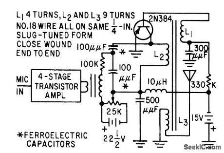
Used two voltage-tunable ferroelectric capacitors. Can be built in pocket-size plastic case when powered with hearing-aid batteries.-T. W. Butler, Jr., Ferroelectrics Tune Electronics, Circuits, Electronics, 32:3, p 52-55. (View)
View full Circuit Diagram | Comments | Reading(683)
WINDOW_DETECTOR_1
Published:2009/7/14 23:05:00 Author:Jessie

Unique voltage-range sensing circuit provides positive indications of high, low or acceptable input levels for voltage and includes adjustments for both threshold and hysteresis levels. R1 and R2 ad just upper and lower thresholds, while R3 and R4 adjust upper and lower hysteresis levels. If acceptable input range is 4.5 V to 5.5V, output of opamp A1 goes negative when ein is greater than 5.5V. This saturates Q1 and Q2, making Q2 output go from 5 V to 0. TTL then indicates that input has exceeded 5,5 V. Upper hysteresis keeps A1 output negative until input has dropped to setting of R3, which might be 5.3 V. Similarly, when input drops below 4.5 V, output of A2 goes positive and saturates Q3.-I. KrellAnalogMonitor Has Threshold and Hysteresis Controls, EDN Magazine, Aug.1, 1972, p 58. (View)
View full Circuit Diagram | Comments | Reading(1415)
FLIP_FLOP_FOLLOWER_FOR_COUNTER
Published:2009/7/14 20:43:00 Author:May
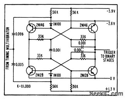
Used to count down cycles of timing mvbr. Output of flip-flop follower is used in and circuit with matrix gates to turn on tone-burst oscillators or multivibrators during positive half-cycles only.-R. W. Rochelle, Cyclops Cores Simplify Earth-Satellite Circuits, Electronics, 31:9, 56-63. (View)
View full Circuit Diagram | Comments | Reading(1108)
TRANSCEIVER_SAVER
Published:2009/7/14 23:05:00 Author:Jessie

Simple circuit has no effect on normal operation of CB transceiver or other solid-state equipment in auto but provides overvoltage protection if voltage regulator in auto fails. Use heatsink with transistor if transmit current is above 2 A. Choose resistance value to give output of 12.6 V during normal operation.-Circuits, 73 Magazine, March 1977, p 152. (View)
View full Circuit Diagram | Comments | Reading(1346)
ACTIVE_REDUNDANI_D_C_AMPLIFIER
Published:2009/7/14 20:43:00 Author:May

Test carrier signal is added to input of normal amplifier A1. When failure occurs in A1, detector senses absence of test catt'1et and causes relay K to change over to amplifier A2. Both amplifiers ore differential type, having open-loop gain of1,000 and closed-loop gain of 10. Open-loop response is flat to about 2kc, and closed-loop response ex tends beyond 5 kc.-T. B. Hooker, Designing Redundant Analog Amplifiers, EEE, 13:2, p 55-59. (View)
View full Circuit Diagram | Comments | Reading(738)
LOW_COST_IC_TUNER
Published:2009/7/14 23:04:00 Author:Jessie
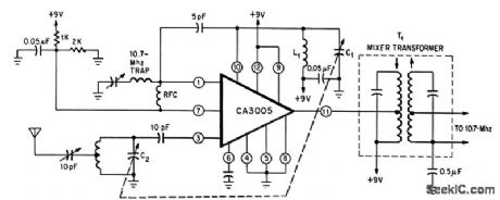
Front end uses single RCA three-transistor two-diode chip with conventional tuning circuit. Ganged capacitors C1.C2 are 5-22 pf. Power gain is 15 db and sensitivity is 10 microvolts for 30 db of quieting. Performance is just adequate for low-cot commercial f-m tuner.-R. L. Sanquini, Integrated Circuits Make A Low-Cost F-M Receiver, Electronics, 39:16, p 133-138. (View)
View full Circuit Diagram | Comments | Reading(1350)
058_TO_465_MICROSEC_DELAY
Published:2009/7/14 23:04:00 Author:Jessie

Saturated germanium transistors give variable time delay for 27-V input pulse having 2.75-microsec width, with R2 controlling delay time and R1 controlling output pulse width.-R. H. Blumenthal and F. E. Williams, Transistor's Stored Charge Controls Pulse Delay, Electronics, 37:19, p 52-53. (View)
View full Circuit Diagram | Comments | Reading(1040)
TOUCH_TONE_DECODER
Published:2009/7/14 20:42:00 Author:May

Uses seven National LM567 phase-locked loop decoders (U1-U7) having high noise rejection, immunity to false signals, and stable center frequency. Each 567 activates proper gate of SN7402, making output of gate go to high or 1 state for driving NPN transistor that can turn on LED labeled with corresponding Touch-Tone number. Alternatively, gate outputs can drive 12 relays, with relay contacts going to LEDs and/or to keyboard switches of ordinary calculator used as display display. Article tells how to adjust 10K pot for each 567 for detection of desired frequency.-W. Mac-Dowell, Touch-Tone Decoder, 73 Magazine, June 1976, p 26-27. (View)
View full Circuit Diagram | Comments | Reading(3375)
TWO_FET_CASCODE
Published:2009/7/14 23:04:00 Author:Jessie

Gives high audio voltage gain (40 db), high impedance, low-noise operation, and good temperature stability with low supply voltage. Q3 serves as loadresistance.-B. Smith, Low-Noise FETs Sound Good To Circuit Designers, Electronics,37:31, p 58-62. (View)
View full Circuit Diagram | Comments | Reading(1120)
PLL_FSK_DEMODU_LATOR
Published:2009/7/14 23:04:00 Author:Jessie

Signetics NE560N phase-locked loop is used as receiving converter for demodulating carrier shifted between two preset frequencies, one corresponding to 0 and other to 1 of binary data signal. PLL provides shifting DC voltage to initiate 1 or 0 (mark or space) code elements. Circuit locks on and tracks output frequency of receiver. Input at pin 12 should be from 30 mV to 2 V P-P square or sine wave. Output of about 60 mVDC at pin 9 is amplified, conditioned, and fed to μA710 comparator to provide proper output voltages for interfacing with printer- Signetics Analog Data Manual, Signetics, Sunnyvale, CA, 1977, p 844-845. (View)
View full Circuit Diagram | Comments | Reading(622)
LINEAR_OUTPUT_RAMP
Published:2009/7/14 20:42:00 Author:May
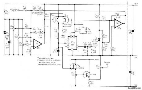
Provides high frequency stability as required for use in sound synthesizers. Can be synchronized to another oscillator. Uses 555 timer in astable mode, with Tr1a supplying constant current to C2. R12 and R13 should be multiturn pots. Synchronizing square-wave signal having 5-10 V peak can be fed in at R19 for differentiation, and resulting spikes used to control threshold voltage of 555. R4 sets minimum frequency. R22 sets average Output level to 0 V R2 and R3 serve as coarse and fine frequency controls Tr1 can also be BFX11 or BFX36. –T. W. Stride, Voltage Controlled Oscillator Wireless World, Oct . 1977, p 66.
(View)
View full Circuit Diagram | Comments | Reading(1216)
5_V_CROWBAR
Published:2009/7/14 23:03:00 Author:Jessie

Simple overvoltage protection circuit for 5-V 1-A logic supply can be adjusted to trigger at 10% overvoltage or 5.5 V. Tunnel diode CR1 senses level. At 5.5 V, diode switches slightly past its valley piont, and voltage across diode biases Q1 into saturation. Q1 then supplies gate current to SCR Q2, which fires and continues conducting until power supply is disconnected. Power supply must include current-limiting circuit and fuse. R3 adjusts trip point.-L. Strahan, Logic-Supply Crowbar, EDN|EEE Magazine, Nov. 15, 1971, p 51. (View)
View full Circuit Diagram | Comments | Reading(2247)
VELOCITY_RESPONSE_PHONO_PREAMP
Published:2009/7/14 23:03:00 Author:Jessie
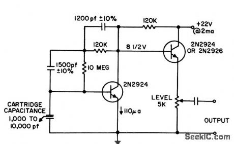
Designed for use with wide range of ceramic cartridge capacitances. Input impedance, which is 30K at 40 cps, decreases with increasing frequency to give velocity response from cartridge, so that preamp frequency response is like that required for a magnetic cartridge. Output is equalized within 1.6 db from 40 cps to 12 kc.- Transistor Manual, Seventh Edition, General Electric Co., 1964, p 258. (View)
View full Circuit Diagram | Comments | Reading(1613)
TRIAC_SUPPRESSES_RELAY_ARCING
Published:2009/7/14 23:02:00 Author:Jessie

Circuit prevents arcing at contacts of relay for loads up to 50 A, by turning on as soon as it is fired by gate current; this occurs after S1 is closed but before relay contacts close. Once contacts are closed, load current passes through them rather than through triac. When S1 is opened, triac limits maximum voltage across relay contacts to about 1 V. Circuit permits use of smaller relay since it does not have to interrupt full load current.- Circuit Applications for the Triac, Motorola, Phoenix, AZ, 1971, AN-466, p 8. (View)
View full Circuit Diagram | Comments | Reading(932)
±15_TO_±75_V_THRESHOLD
Published:2009/7/14 23:02:00 Author:Jessie

Precise timing and accurate threshold levels are assured by stable characteristics of input differential amplifier in CA 3080 variable opamp used to drive one of inverter/amplifier transistors in CA3600E array. For values shown, threshold voltage for given polarity is half of supply voltage used, in range of 3 to 15 V.- Circuit Ideas for RCA Linear ICs, RCA Solid State Division, Somerville, NJ, 1977, p 16. (View)
View full Circuit Diagram | Comments | Reading(607)
REGULATOR_OVERLOAD
Published:2009/7/14 23:00:00 Author:Jessie

When output is shorted, germanium diode D1 turns on and draws current through R1, removing reference voltage across zener. Tr1 is then held off and turns Tr3 and Tr4 off to block load current. When short is removed, circuit recovers automatically.-D. E. Waddington Germanium Diode for Regulator Protection, Wireless World, March 1977, p 42. (View)
View full Circuit Diagram | Comments | Reading(1232)
CONTROL_FOR_VOLTAGE_TUNED_OSCILLATOR
Published:2009/7/14 20:39:00 Author:May

Input d-c control voltage required by SiC varistors of voltage-tuned oscillator is boosted by d-c amplifier stages that produce two control voltages (at A and B) for SiC varistors of phase-shift oscillator circuit, changing their a-c resistance and thereby oscillator frequency.-M. Uno, Varistor Network Controls Voltage-Tuned Oscillator, Electronics, 34:30, p 44-47. (View)
View full Circuit Diagram | Comments | Reading(901)
LOW_LEVEL_LOW_NOISE_HIGH_GAIN
Published:2009/7/14 23:00:00 Author:Jessie

Gives gains up to 1,000(60 db) for high-impedance,transducer applications, With typical noise figure of 1 db at emitter currents below 1 microamp and generator resistance above 1 meg. Such performance was previouslyavailable only with vacuum tubes and field-effect transistors. Ideal for spaceapplications.-Texas Instruments Inc., Solid .State Communications, McGraw-Hill,N.Y., 1966, p 291. (View)
View full Circuit Diagram | Comments | Reading(1155)
DEMODULATOR_FOR_170_Hz_SHIFT
Published:2009/7/14 22:59:00 Author:Jessie

Converts RTTY audio tones of 2125 and 2295 Hz to DC pulses required for driving selector magnets of teleprinter. Coupling Iinks are added to standard 88-mH toroids as indicated.-I Schwartz, An RrrY Primer,CQ, Feb 1978,P 31-36. (View)
View full Circuit Diagram | Comments | Reading(575)
| Pages:606/2234 At 20601602603604605606607608609610611612613614615616617618619620Under 20 |
Circuit Categories
power supply circuit
Amplifier Circuit
Basic Circuit
LED and Light Circuit
Sensor Circuit
Signal Processing
Electrical Equipment Circuit
Control Circuit
Remote Control Circuit
A/D-D/A Converter Circuit
Audio Circuit
Measuring and Test Circuit
Communication Circuit
Computer-Related Circuit
555 Circuit
Automotive Circuit
Repairing Circuit