
Circuit Diagram
Index 619
DTMF_INFRARED_TRANSMITTER
Published:2009/7/14 7:21:00 Author:May
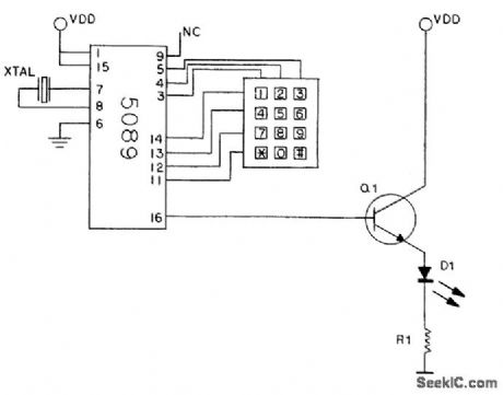
This transmitter uses a 5089 DTMF generator chip and a keypad to generate DTMF signals and modulate them on an IR light beam from an IR LED. Xtal is a 3.579-MHz TV burst crystal. (View)
View full Circuit Diagram | Comments | Reading(5680)
IMPEDANCE_CONVERTER
Published:2009/7/14 7:18:00 Author:May

This circuit is a high-input-impedance-to-low-output-impedance converter circuit with unity voltage gain. In the circuit, an LM741 op amp, U1, is connected in a voltage-follower circuit that drives a complementary transistor-emitter-follower circuit. The output of the circuit can be used to drive low-current lamps, relays, speakers, etc. The feedback can be taken from the output to pin 2 of the LM741 if it is desired to include Q1and Q2 in the feedback loop. (View)
View full Circuit Diagram | Comments | Reading(0)
NEGATIVE_IMPEDANCE_CONVERTER
Published:2009/7/14 7:17:00 Author:May

Recall that a resistor is a voltage-dependent current consumer; this circuit does the opposite.If you connect a battery to its input, the battery will get charged, with exactly the current that the battery would have delivered if you had connected it to a 1000-Ω resistor. If you put a 1000-Ωresistor in parallel with a 1000-Ω NIC, you'll get what looks like an infinite resistance. No matter what voltage you apply (within limits), the NIC will match it, and all the current flowing in the resistor will come from the NIC, not from the externally applied voltage. (View)
View full Circuit Diagram | Comments | Reading(0)
PINK_NOISE_GENERATOR
Published:2009/7/14 7:15:00 Author:May

The MM5837 is a digital white-noise generator IC. It produces a clean white noise signal with only a power source. White noise appears at the output of this IC when power is applied. The white-noise signal is then fed through a -3-dB/octave filter to give pink noise. Because the minimum rolloff with a single-stage RC (resistor/capacitor) filter is -6 dB/octave (because of capacitive reactance), an unconventional filter design is needed. The technique involves cascading several stages of lag compensation so that the zeros of one stage partially cancel the poles of the next stage. The result is shown in the schematic of the figure. The response of this circuit is accurate to within ±1/2 dB. (View)
View full Circuit Diagram | Comments | Reading(0)
SYNTHETIC_PUSH_PULL
Published:2009/7/15 2:29:00 Author:Jessie

Single transistor in sliding class-A output requires no input transformer, while approximating push-pull class-B output stage.-J. A. Worcester, One. Transistor Push-Pull, Electronics, 32:24, p 74. (View)
View full Circuit Diagram | Comments | Reading(1082)
100_350_CPS_RECEIVER
Published:2009/7/15 2:28:00 Author:Jessie

Input signal from electrodes of crevasse detector is attenuated to suitable level at constant impedance of 1,000 ohms by T-pad and passed to 2N107 preamplifier whose supply voltage is stabilized at 5.8 v by reversed 71620 silicon diode shunt operating at zener point. Signal is then fed through bandpass L-C filter to amplifier, driver, and final 355 class A stage that drives recorder pen motor and relaymeler.-H. P. Van Eckhardt, Crevasse Detector Blazes Glacial Trails, Electronics, 31:3, p 63-65. (View)
View full Circuit Diagram | Comments | Reading(958)
400_W_60_CPS_DUAL_TRANSFORMER_IN_VERTER
Published:2009/7/15 2:28:00 Author:Jessie

Input voltage is divided equally among four series primaries so each transistor is subjected only to 60 v when off. Output is 140-v square wave. Efficiency is 95% at full load. Use of dual-transformer configuration makes frequency of oscillation easy lo adjust by changing setting of RF, to give exactly 60 cps for any value of load cur rent.-Texas Instruments Inc., Transistor Circuit Design, McGraw-Hill, N.Y., 1963, p 459. (View)
View full Circuit Diagram | Comments | Reading(639)
TOUCH_TON_E_ENCODER
Published:2009/7/14 6:14:00 Author:May
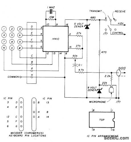
Crystal-controlled encoder using 14410 tone encoder operates from 12-V supply to provide good frequency stability along with correct balance between high and low tones. 50K level adjustment pot can be screwdriver type.-G. A. Wilson, The Micoder: Some Improvements, Ham Radio, Nov. 1978, p 42-43. (View)
View full Circuit Diagram | Comments | Reading(1055)
TRUE_RMS_DETECTOR
Published:2009/7/15 2:25:00 Author:Jessie

Circuit using National LM118 opamps provides DC output equal to RMS value of sine, triangle, square, or other input waveform with 2% accuracy for 20 V P-P inputs from 50 Hz to 100 kHz. Circuit is usable up to about 500 kHz but with lower accuracy. Direct coupling of input provides true RMS equivalent of combined DC and AC signals. Absolute-value amplifier A1 provides positive input current to A2 and A4 independent of signal polarity. Amplifiers A2-A5 and transistors Q1-Q4 form log multiplier/divider. To calibrate, 10-VDC input signal is applied and R10 is adjusted for 10-VDC output. Transistors should be matched and mounted on common heatsink if possible.-R. C. Dobkin, True RMS Detector, National Semiconductor, Santa Clara, CA, 1973, LB-25.
(View)
View full Circuit Diagram | Comments | Reading(0)
BELL_SIMULATOR
Published:2009/7/14 6:08:00 Author:May

Uses AMI S2561 CMOS IC to simulate effects of telephone bell by producing tone signal that shifts between two predetermined frequencies at about 16 Hz. In applications where dial pulse rejection is not necessary, network inside dashed lines can be omitted and pins EN and D1 connected directly to VDD, which is typically 10V. Power is derived from telephone lines by diode-bridge supply. Values shown give tone frequencies of 512 and 640 Hz. Power output to 8-ohm loudspeaker is at least 50 mW, fed through 200:8 ohm trans-former.- Tone Ringer, American Microsystems, Santa Clara, CA, 1977, 52561, p 1. (View)
View full Circuit Diagram | Comments | Reading(931)
QUICKBROWN_FOX_GENERATOR
Published:2009/7/15 2:24:00 Author:Jessie

TTL ICs and National MM5220DF preprogrammed MOS read-only memory chip together generate standard RTTY test message:THE QUICK BROWN FOX JUMPS OVER THE LAZY DOG 1234567890 DE. Requires external clock providing sharp negative-going pulse train at frequency corresponding to RTTY speeds desired Requires two supplies, for +5 V and 112 V.-K. Ebneter and J. Romelfanger, RTTY Test-Message Generator, Ham Radio, Nov. 1976, p 30-32. (View)
View full Circuit Diagram | Comments | Reading(769)
PEAK_TO_PEAK_VOLTMETER
Published:2009/7/15 2:23:00 Author:Jessie

Two Optical Electronics opamps and two peak sense-andhold modules form positive-peak-sense memory that adds negative peak amplitude to entire signal so as to bias negative peak to zero. Input must be restricted to ±5 V full scale (10 V P-P). Output is 0 V for -5 V input and +10 V for +5 V input. Unsymmetrical signals such as +2 V to -8 V still give +10 V output.- Using Peak Sense Memories as Peak-to-Peak Detectors, Optical Electronics, Tucson, AZ, Application Tip 10275. (View)
View full Circuit Diagram | Comments | Reading(735)
LOGARITHMIC_INPUT_CURRENI_COMPRESSOR
Published:2009/7/14 6:07:00 Author:May

Simple d-c logarithmic amplifier compresses positive input current into logarithmically related input voltage.-G. W. Candel, D-c Logarithmic Amplifier Compresses Input Current, Electronics, 39:10, p91-92. (View)
View full Circuit Diagram | Comments | Reading(710)
200_W_60_CPS_115_V_POWER_FROM_12_V
Published:2009/7/15 2:22:00 Author:Jessie

Uses saturating-core oscillator. Complete design procedure is given. maximum frequency drift is below 0.5% for change from no load to full load and for input change from 11.5 to 13.5 v. Efficiency is about 86%.No.load input power is 8.5 w.-Texas instruments Inc., Transistor Circuit Design, McGraw-Hill, N.Y., 1963, p 451. (View)
View full Circuit Diagram | Comments | Reading(709)
DIAL_TONE_GENERATOR
Published:2009/7/14 6:07:00 Author:May

Simultaneous pairs of Touch-Tone frequencies used by telephone company are generated by adjustment-free circuit using Motorola Touch-Tone dialer with extenal 1-MHz crystal. Internal circuits of IC select proper division rates and convert outputs to synthesized sine waves of correct frequencies. Grounding one of row inputs by pressing key gives lower-frequency tone, while grounding one of column inputs gives higher-frequency tone. Special Touch-Tone keyboard provides this grounding action automatically when single key is pressed.-D. Lancaster, CMOS Cook-book, Howard W. Sams, Indianapolis, IN, 1977, p 239-240. (View)
View full Circuit Diagram | Comments | Reading(4803)
METER_OVERLOAD
Published:2009/7/15 2:22:00 Author:Jessie

When used with basic meter movement, circuit ensures that overloads merely make pointer run off scale in either direction in controlled manner and press gently against stop pin instead of winding around pin, Values shown will suit most meter movements, but article gives complete design procedure. If voltage being measured is between 350 and 700 mV, use two diodes in series in each position. For voltages between 700 mV and 1 V, use three diodes in series. Diode types are not critical.-C, Shenton, Meter Protection Circuit, Wireless World, Oct. 1972, p 475. (View)
View full Circuit Diagram | Comments | Reading(788)
LOW_DRIFT_WITHOUT_CHOPPER
Published:2009/7/14 6:05:00 Author:May

Developed for airborne or missile telemetry. Gain is adjustable. Has wide frequency response, high common-mode rejection factor, and high input impedance, along with gain stability of 0.15% over wide temperature range.-R. D Middlebrook and A. D. Taylor, Differential Amplifier with Regulator Achieves High Stability, Low Drift, Electronics, 34:30, p 56-59. (View)
View full Circuit Diagram | Comments | Reading(640)
CALIBRATED_GAIN_AMPLIFIER
Published:2009/7/15 2:21:00 Author:Jessie

Used to extend low range of VOM or CRO and provide very high input impedance (above 1000 megohms), Gain of amplifier from DC up to several hundred kilohertz is determined by ratio of 10K feedback resistor to 200- or 2000- ohm preset pot. Action is noninverting Maximum input voltage range is ±10V Dual battery supply must be used To calibrate, short input test leads and adjust 1-megohm pot for zero on VOM or other indicating instrument.-J. J. Schultz, Versatile Test Equipment Range Extender, 73 Magazine,Nov 1973, p 59-62. (View)
View full Circuit Diagram | Comments | Reading(554)
FET_UNITY_GAIN_D_C_AMPLIFIER
Published:2009/7/14 5:54:00 Author:May
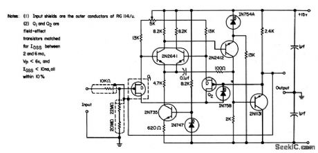
Each base of 2N2641 dual transistor is driven by source follower fet’s Q1 and Q2. Q1 performs impedance transformation, while Q2 closes feedback loop and tends to cancel changes in parameters due to temperature variations.-L. J. Sevin, Jr. Field-Effect Transistors, McGraw-Hill, N.Y.1965, p102. (View)
View full Circuit Diagram | Comments | Reading(704)
UPWARD_SHIFT_RTTY_DEMODULATOR
Published:2009/7/15 2:21:00 Author:Jessie

PLL demodulator serves for copying AFSK/FSK up-ward-shift RTTY signals, 2N706 switches 2N5655 on and off, reversing polarity of voltage from LM741 comparator on mark/hold as needed for smooth upward-shift copy. Works equally well on wide-shift or narrow-shift signals. Zero-center tuning meter will show full-scale minus (left) reading on mark/hold signal Meter may not be needed on AFSK.-N. Stinnette, Update of the Phase-Locked Loop RTTY Demodulator, Ham Radio, Aug. 1976, p 16-17.
(View)
View full Circuit Diagram | Comments | Reading(2473)
| Pages:619/2234 At 20601602603604605606607608609610611612613614615616617618619620Under 20 |
Circuit Categories
power supply circuit
Amplifier Circuit
Basic Circuit
LED and Light Circuit
Sensor Circuit
Signal Processing
Electrical Equipment Circuit
Control Circuit
Remote Control Circuit
A/D-D/A Converter Circuit
Audio Circuit
Measuring and Test Circuit
Communication Circuit
Computer-Related Circuit
555 Circuit
Automotive Circuit
Repairing Circuit