
Circuit Diagram
Index 614
120_VAC_SINGLE_HETEROSTRUCTURE_LASER_DRIVER_SUPPLY
Published:2009/7/14 11:38:00 Author:May

This figure shows the complete schematic of the 120-Vac SH power supply. The circuit consists of a polarized plug, a voltage doubler, a large-value storage capacitor, two neon indicator lamps to show that ac and dc power is present, a 1-MΩ firing-rate control, and the business end of the supply to drive the laser. I2 is also a safety light. When it is on, the laser should be considered operating. The current to the voltage doubler is limited by resistors R1 to R3, and by the capacitive reactance of capacitors C1 and C2. R7-a 47-kΩ, 1/2-W resistor-limits the input power to the avalanche circuit to avoid overheating the diode or Q1. The capacitors and resistors serve to isolate the circuit from the ac line sufficiently to prevent a shock hazard; however, you can still get shocked. Be sure you put this device in a nonconductive case, and obey the polarity of the polarized plug. Don't touch any part of the circuit while it's plugged in, either. Be sure you use a plastic potentiometer for VR1, or a separate control-type potentiometer with a plastic knob. (View)
View full Circuit Diagram | Comments | Reading(1045)
LASER_DIODE_DRIVER
Published:2009/7/14 11:31:00 Author:May

One way to drive a single heterostructure laser diode. The transistor is driven in avalanche mode, producing short-duration pulses of current. (View)
View full Circuit Diagram | Comments | Reading(1087)
LASER_ACTIVATED_RELAY_WITH_AMPLIFIER
Published:2009/7/14 11:30:00 Author:May
A low-noise amplifier is used in conjunction with a phototransistor to allow higher sensitivity than the detector alone would provide. (View)
View full Circuit Diagram | Comments | Reading(774)
DIFFERENTIAL_INPUTS_GIVE_GROUND
Published:2009/7/15 2:53:00 Author:Jessie

REFERENCED OUTPUT-Circuit consists of differential-input controlled-current rectifying source A1-A2 and level-shifting voltage-to-current converter A3. Feedback current of appropriate polarity is conducted to output opamp, while other feedback current is absorbed. Possible drawbacks are switching offset and bandwidth limitations common to precision rectifiers. Article gives design equations and theory of operation.-J. Graeme, Measure Differential AC Signals Easily with Precision Rectifiers, EDN Magazine, Jan. 20, 1975, p 45-48. (View)
View full Circuit Diagram | Comments | Reading(1014)
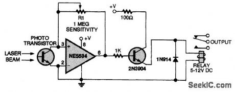
LASER_BEAM_ACTIVATED_RELAY
Published:2009/7/14 11:29:00 Author:May

This two-transistor relay circuit will activate whenever the phototransistor is illuminated by the laser beam. (View)
View full Circuit Diagram | Comments | Reading(1703)
50_MC_TO_100_MC_PUSH_PUSH_DOUBLER
Published:2009/7/15 2:53:00 Author:Jessie
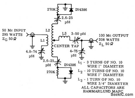
Two 1N4386 varactors are connected in phrase opposition to input signal and parallel to common load at even harmonic signal, to give action comparable to push-push circuit. Power-handling capacity is twice that of single varactor, with added benefit of odd-harmonic suppression.-G. Schaffner and J. Cochran, Varactor Diodes and Circuits for High Power Output and Linear Response, Motorola Application Note AN-191, Aug. 1965. (View)
View full Circuit Diagram | Comments | Reading(759)
NPN_PHONO_PREAMP
Published:2009/7/15 2:53:00 Author:Jessie
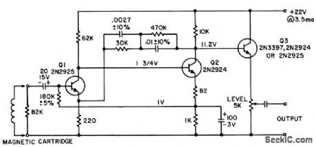
Input of 6 mv at 1 kc from magnetic cartridge gives 1 v output, which is 15 db below clipping level and 72 db above unweighted noise level. RIAA equalized output is within 1 db from 40 cps to 12 kc.- Transistor Manual, Seventh Edition, General Electric Co., 1964, p 257. (View)
View full Circuit Diagram | Comments | Reading(2825)
D_BISTABLE
Published:2009/7/14 11:27:00 Author:May

The interesting point of this circuit is that a D-type bistable is used as an inverter. When the level at the input changes from high to low, the bistable is reset and its Q output goes high. When the input becomes low, the reset is removed and the Q output goes low. The delay introduced by network R1-C1 between the RESET input and the CLOCK input makes it possible to trigger the bistable at the leading edge of the input signal. As an example, in the case of a dual D-bistable Type 74HCT74, the time needed for a clock pulse to be accepted after the reset has been removed is 5 ns. Therefore, an RC introducing a delay of 7.5 ns gives a reasonable safety margin. The reduced edge gradient of the clock pulse does not create any problems because the maximum allowed rise time of the clock input is 500 ns. To obviate asymmetrical output signals, it is advisable to limit the input frequency to about 1 MHz with component values as specified. (View)
View full Circuit Diagram | Comments | Reading(910)
REGULATED_LOW_NOISE_VOLTAGE_INVERTER
Published:2009/7/14 11:25:00 Author:May

Analog cell phones rely on a quiet GaAsFET bias supply to maximize the signal-to-noise ratio, providing a high-quality transmission. The LTC 1551CS8-4. 1 switched-capacitor voltage inverter circuit shown reduces output noise to less than 1 mV on the -4.1-V regulated output voltage. The 900-kHz operating frequency allows the charge pump to use small 0.l-μF capacitors. The 10-μF and 0.1-μF output capacitors effectively reduce the 900-kHz ripple noise to relatively insignificant levels. The LTZ1550CS8-4.1 has an active low shutdown input (SHDN), whereas its counterpart, the LTC1551CS8-4.1, has an active high shutdown input. This choice minimizes component count.The LTC1550 and 1551CS8-4.1 both operate in doubler mode, meaning that they only invert the input voltage and regulate it down to -4.1 V. The input voltage range is 4.5 to 7 V. (View)
View full Circuit Diagram | Comments | Reading(637)
CRYSTAIVFO_SYNC_GENERATOR
Published:2009/7/15 2:52:00 Author:Jessie
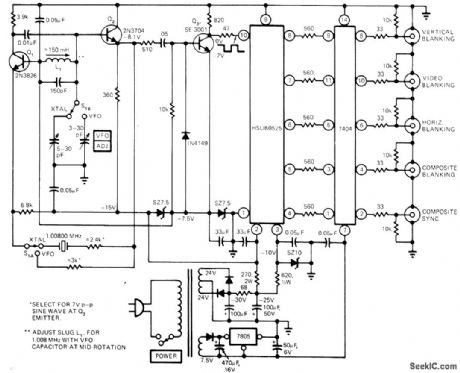
With crystal, can be used as system sync generator or as drive for staircase generators, custom pattern generators, and special TV test equipment. When VFO-controlled, circuit provides variable-frequency sync needed for determining pull-in range of sweep oscillators in TV sets and VTR decks. Clock-pulse section uses Q1 and Q2 as 1.00800-MHz Butler oscillator. On VFO operation, oscillator frequency can be varied ±3.5% from mean. Sine-wave output of Q2 is converted to square wave by Q3 for application to clock input of Hughes HSUB0525 sync generator. Each output of sync generator feeds one of inverters in 7404, providing 3.3 V P-P signal into 75-ohm load for each output.-M. J. Salvati, VFO Adds Versatility to TV Sync Generator, EDN Magazine, May 20, 1974, p 70 and 72. (View)
View full Circuit Diagram | Comments | Reading(2575)
GATE_INVERTERS
Published:2009/7/14 11:22:00 Author:May

Logic gates can be configured as buffers or inverters as shown. (View)
View full Circuit Diagram | Comments | Reading(605)
AC_PEAKS
Published:2009/7/15 2:52:00 Author:Jessie
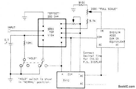
Optical Electronics 5893 peak sense-and-hold analog memory module senses input peaks of AC waveforms and produces smooth DC output voltage for driving 21/2 -digit digital voltmeter. Output of 5893 is divided by about 10 to give 1-V full-scale output for meter. External capacitor used with parallel resistor provides time constant required for steady display on DVM. Response time is 4 s for input change from 10 V to 0 and less than n s for rise from 0 to 10 V. Useful bandwidth is 20 Hz to 2 MHz. HOLD switch is operated when peak reading on meter is to be held several minutes.- Digital Peak Reading AC Voltmeter, Optical Electronics, Tucson, AZ, Application Tip 10259. (View)
View full Circuit Diagram | Comments | Reading(1200)
CORDLESS_HEADPHONES
Published:2009/7/14 11:21:00 Author:May

It is possible to use headphones with no direct connection to the audio source. This figure illustrates a simple transmitter circuit suitable for connecting to an audio source. Diodes D1 to D3 are three infrared LEDs in series, driven by TR2, an n-channel MOSFET with a drain-current rating of 500 mA maximum. The illumination of the LEDs is modulated by the audio signal applied, with TR1 current-limiting and shunting the bias of TR2 to ground when TR2 source current exceeds roughly 100 mA. Potentiometer VR1 should be adjusted for best results. A 9-V power supply is best used in this circuit because of the sustained level of current consumption. The transmitter range is about 1 to 2 m, but this can be extended by using reflectors behind the diodes.A suggested receiver circuit, using an infrared photodiode, D4, to detect the IR light, is shown in (b). The received signal is ac-coupled to TR3, another MOSFET. The output is taken from the drain terminal via capacitor C5. Bias can be adjusted with potentiometer VR2, and this circuit will run from a PP3-size battery. The circuit could be adapted for other applications.
(View)
View full Circuit Diagram | Comments | Reading(1604)
IR_RELAY_CIRCUIT
Published:2009/7/14 11:17:00 Author:May

All IR is received by the module via an IR photodiode. The diode is operated in its reverse-bias current it permits depends on the intensity of the received infrared light. The fluctuations in the reverse-bias current are then amplified by a high-gain stage. The output of the amplifier is then limited by the next stage. The limiter chops the extreme highs and lows off the amplified signal, and the result is a quasi-digital pulse train. The simplified wave then passes through a bandwidth filter that has its center frequency at 40 kHz. At that point, the circuit has effectively retrieved the 40-kHz remote carrier. The reproduced carrier is then integrated. The next stage is an inverting Schmitt trigger. It will not go low unless the filter's output signal surpasses a certain amplitude, and it will not go high again until the signal drops below a certain minimum. Thus, the Schmitt trigger responds only to large changes in the filter's output (caused by bursts and pauses) and ignores small changes (caused by the 40-kHz carrier, to which the filter can't respond quickly). The Schmitt trigger's output is thus low when a 40-kHz burst is received, and high during pauses between bursts. The resulting waveform is an inverted version of the pulses that were modulated and transmitted by the remote. The oscillator circuit is based on a 555 timer. With D3, R2 is bypassed (or shorted out) while C1 is charging, but is in the current path during discharge. Therefore, with R1 and R2 made equal, the charge time equals the discharge time, yielding an output with a 50-percent duty cycle. Components R1, R2, and C1 (all precision, drift-free units) have been chosen to provide a 40-kHz output in this configuration. That output strobes the IR LEDs via Q1. The oscillator functions only when pin 4 of the 555 is high. Because that pin is connected to the inverter circuit, the oscillator functions when the inverter's input is low. The inverter's input is connected to MOD1's output, which goes low with each remote burst received. So overall, the circuit produces a 40-kHz IR burst when it receives one. (View)
View full Circuit Diagram | Comments | Reading(1836)
IR_REMOTE_CONTROL_RECEIVER_1
Published:2009/7/14 11:11:00 Author:May

The figure shows a schematic of the IR receiver circuit. The heart of the circuit is MOD1, an infrared detector module that removes the IR carrier frequency and transmits only the data that are encoded in the received IR signal. A suitable IR module is available at Radio Shack (No. 276-137).The IR module needs a clean 5-V power supply, which is provided by IC1, a 7805 regulator. Power is supplied to the regulator by 9-V battery B1. The output of the module is wired to a male DB-25 multipin connector. The infrared detector module receives a signal, filters it, and removes the 40-kHz carrier. The output of the module is a TTL-level signal consisting of long and short pulses. The PC records those voltage levels over time, while the signal is being sent, and stores the data in a file. The line normally used by the PC's printer port to indicate that the printer is out of paper (pin 12) is used in this project to accept data from the IR module. The I/O port is located at the address ox379. Bit 5 corresponds to input pin 12. Various software programs are required to let a PC store information input to its printer port. (All of the software is available on the Gernsback BBS-516-293-2283, v.32, v.42bis-contained in a file called IR-TEST.ZIP.) The source code of the first program, IRLOG.EXE, is written in C. The program stores the value it reads from the PC's printer port into an array. When the input line is logic high, the ASCII character 1 is stored in the array. When the input line is logic low, ASCII character 0 is stored. (View)
View full Circuit Diagram | Comments | Reading(1199)
IR_REMOTE_CONTROL_MODEL_RAILROAD_APPLICATION
Published:2009/7/14 11:06:00 Author:May

This circuit can be used to interface two triacs to the IR remote control in order to control model railroad track switches. (View)
View full Circuit Diagram | Comments | Reading(694)
50_MC_TO_200_MC_VARACTOR_QUADRUPLER
Published:2009/7/15 2:51:00 Author:Jessie
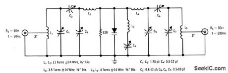
Uses 1N4386 varactor capable of handling 50 w input power up to 300 Mc. Gives efficiencies up to 70%.-G. Schaffner, High Power Varactor Diodes, Motorola Application Note AN-147, Apr. 1964. (View)
View full Circuit Diagram | Comments | Reading(716)
50_350_MICROSEC_BOOTSTRAP_DELAY
Published:2009/7/15 2:51:00 Author:Jessie

Provides continuously variable delay. Requires mvbr to generate necessary gate, and two amplifier stages following comparator diode to sharpen output waveform.-NBS, Hand-book Preferred Circuits Navy Aeronautical Electronic Equipment, Vol. 1, Electron Tube Circuits, 1963, p N9-2. (View)
View full Circuit Diagram | Comments | Reading(534)
SEE_THROUGH_SENSOR
Published:2009/7/14 11:02:00 Author:May
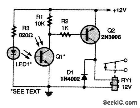
In this circuit, an infrared emitter LED (LED1) is aimed at an infrared phototransistor (Q1). As long as the IR light path between the two remains uninterrupted, transistor Q2 will keep relay RY1 closed. Any opaque object blocking the light path will cause RY1 to open. This circuit is a see-through-type light sensor. Such units are often used as part-in-place detectors and parts-counter sensors. (View)
View full Circuit Diagram | Comments | Reading(4151)
COMMON_BASE_UHF_AMPLIFIER_OR_DOUBLER
Published:2009/7/15 2:51:00 Author:Jessie

With output tank circuit tuned to frequency input, power gain ranges between 10 and 16 db for 40 to 1,000 Mc, with band-width varying from 10 to 40 Mc depending on temperature, frequency, and loading. Tuning tank to twice input frequency gives frequency doubler.-A. E. Munich, Basic UHF Circuit Forms Amplifiers and Multipliers, Electronics, 37:20, p 59-60. (View)
View full Circuit Diagram | Comments | Reading(1139)
| Pages:614/2234 At 20601602603604605606607608609610611612613614615616617618619620Under 20 |
Circuit Categories
power supply circuit
Amplifier Circuit
Basic Circuit
LED and Light Circuit
Sensor Circuit
Signal Processing
Electrical Equipment Circuit
Control Circuit
Remote Control Circuit
A/D-D/A Converter Circuit
Audio Circuit
Measuring and Test Circuit
Communication Circuit
Computer-Related Circuit
555 Circuit
Automotive Circuit
Repairing Circuit