
Circuit Diagram
Index 601
WIND_DIRECTION_SENSOR
Published:2009/7/15 0:11:00 Author:Jessie
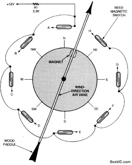
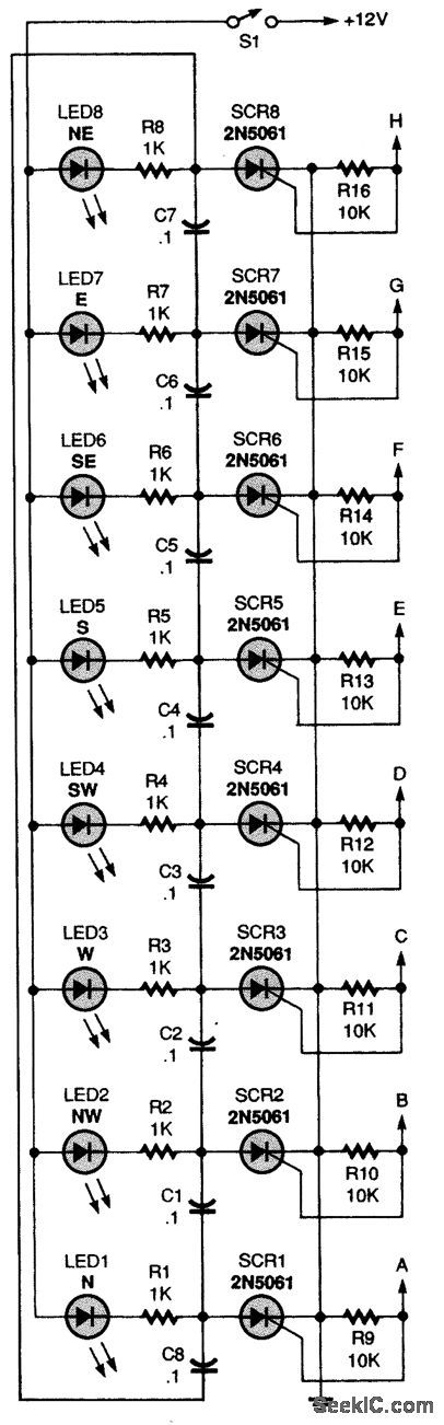
To use the circuit you will need a wind vane like the one shown. It should have a weighted front end and an air paddle in the rear. Attach a small, strong magnet to the front part of the wind-vane arm. Then, position eight reed magnetic switches in a circle around a piece of plastic pipe and electrically connect them (as shown). Note that the reed switches are electrically connected to points labeled A through H. Those points correspond to points A through H in the wind-direction decoder circuit. The decoder uses eight low-current 2N5061 SCRs and eight LEDs to latch and display the wind vane's position. If the wind vane is pointing due north, reed switch A is closed, sending current into the gate of SCR1. That current turns the thyristor on, causing it to light LED1. If the wind shifts slightly to a position in between north and northwest or north and northeast, without activating any of the reed switches, LED1 will remain on, indicating that the last wind direction was north. With SCR1 turned on, one end of capacitors C8 and C1 is pulled to ground. The other end of both capacitors is tied to the + 12-V bus through a resistor and LED; that means that both capacitors are charged to near 12 V. All other capacitors are not charged because both ends of each capacitor are returned to the +12-V bus through a resistor and LED. When the wind direction shifts to the northwest, reed switch B turns SCR2 on, thereby taking the positive end of C1, which is connected to its anode, to ground. This negative pulse turns SCR1 off as SCR2 turns on, lighting LED2 and turning off LED1. (View)
View full Circuit Diagram | Comments | Reading(8699)
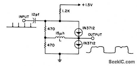
PCM_DECODER
Published:2009/7/15 0:05:00 Author:Jessie

Three CMOS ICs provide decoding of Manchester (split-phase) PCM signals by generating missing mark which should occur NRZL at each change of level data to recover original clock frequency. Retriggerable mono MVBR NHZL times out at slightly longer than half of original clock frequency. Signal levels are TTL-compatible. Values of C and R depend on system frequency. Other resistors are 15K, and other capacitors are 470 pF.-M. A. Lear, M. L. Roginsky, and J. A. Tabb, PCM Signal Processor Draws Little Power, EDN Magazine, April 20, 1975, p 70. (View)
View full Circuit Diagram | Comments | Reading(4848)
PULSE_STRETCHING__MONO
Published:2009/7/15 0:02:00 Author:Jessie

Section of CMOS MM74C04 inverter accepts positive input pulse by going low and discharging C. Capacitor is rapidly discharged, driving input of MM74C14 Schmitt trigger low. Output of Schmitt then goes positive for interval To which is equal to input pulse duration plus interval T that depends on values used for R, C, and supply voltage.- CMOS Databook, National Semiconductor, Santa Clara, CA, 1977, p 5-30-5-35. (View)
View full Circuit Diagram | Comments | Reading(1140)
VACUUM_TUBE_TRANSMITTER
Published:2009/7/14 21:11:00 Author:May
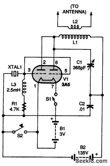
The schematic for the transmitter is shown in the figure. In the circuit, power is supplied by a 3V battery B1 and a 135-V battery B2. The latter battery, B2, can be replaced by a power-supply circuit. Switch S1 is used to turn the circuit on and off. The heart of the circuit is a 3A5 tube, V1. Both sections of V1 are connected in parallel in a conventional Miller oscillator. Resistor R1 sets the bias for the tube; the value of R1 might seem low to some because it is only 4700Ω, but keep in mind that V1 is a transmitting triode operating at class C. A 2.5-mH RF choke coil (L3) is needed to keep the radio frequency where it belongs. Capacitor C1 and inductor L1 resonate at the frequency of a 40-m (7- to 7.3-MHz) amateur crystal, XTAL1. Inductor L2 couples RF energy to an attached antenna; C2 is a bypass capacitor. Switch S2 is a telegraph-type key switch. That is used to generate the content of any transmissions you make. Transformer T1 provides isolation from the power line. The isolated ac voltage is rectified by diode D1 and filtered by capacitor C1. (View)
View full Circuit Diagram | Comments | Reading(3559)
TWO_STAGE_CASCADED_COMMON_EMITTER
Published:2009/7/15 Author:Jessie

Design procedure is given for low-level amplifierthat is one of the most-used circuits in all transistor applications, for boosting milli-volt-range signals to workable level of several volts. Capacitance coupling isused for ac operation along with d-c stability. Total power gain is 64 db. Voltagegain is 1,000.-Texas Instruments Inc., Transistor Circuit Design, McGraw. Hill,N.Y.,1963, p 198. (View)
View full Circuit Diagram | Comments | Reading(2814)
FEEDBACK_PROVIDES_STABILIZATION
Published:2009/7/14 21:11:00 Author:May

Resistor Rf, connected between bases of Q1 and Q2, provides negative feedback to make flip-flop less sensitive to voltage variations and transistor unbalance. Will operate on 3.v pulses having 0.5-microsec fall time. Without feedback, higher voltage would be required for triggering.-P. Cheilik, Feed-back Stabilizes Flip-Flop, Electronics, 31:19, p 91-96. (View)
View full Circuit Diagram | Comments | Reading(546)
12_V_AUDIO_AMPLIFIER
Published:2009/7/14 23:59:00 Author:Jessie

Input sensitivity is 10 to 20 mv for 0.5 w output. Maximum power output at 10% harmonic distortion is 500 mw. Design calculations are given.- Transistor Manual, Seventh Edition, General Electric Co., 1964, p 246. (View)
View full Circuit Diagram | Comments | Reading(774)
SINGLE_TONE_SIGNALING
Published:2009/7/14 21:11:00 Author:May

Wien-bridge oscillator using 741 opamp drives 2N2924 or equivalent NPN transistor to generate stable audio tone for signaling over telephone lines Tuning capacitor(C2 and C3 are equal)and resistor(R2 and R3 are equal) values range from 0.1μF and 15.9K for 100 Hz to 0.005 μF and 6.3K for 5000Hz For other frequencies use f =0.159/R2C2 With 12-V supply tone output is about 7 V P-P Select R7 to match impedance of driven circuit.-C. D Rakes. Integrated Circuit Projects. Howard W Sams . Indianapolis IN 1975.p 55-60. (View)
View full Circuit Diagram | Comments | Reading(1273)
12_W_TRANSFORMERLESS_AMPLIFIER
Published:2009/7/14 23:56:00 Author:Jessie

Uses two transistors in parallel for each of theoutputs, to cut saturation resistance in half and thereby increase power output.Parallel operation also serves to reduce distortion. Operating efficiency is 67% at 12 w.- Transistor Manual, Seventh Edition, General Electric Co., 1964, p 267. (View)
View full Circuit Diagram | Comments | Reading(628)
TELEMETRY_SUMMING_AMPLIFIER
Published:2009/7/14 21:10:00 Author:May

Uses differential dual-triode first stage, voltage amp lifer, and current and voltage-limited cathode follower to give output swing of 5V above and below 0. Open loop gain of 2,000 is obtained with positive feedback in last two stages. Used to isolate transducers and to amplify d-c or low-frequency signals in air. borne or ground-based telemetry systems.-L. S. Klivans, D-C Amplifiers for Control Sys terns, Electronics, 31:47, p 96-100. (View)
View full Circuit Diagram | Comments | Reading(846)
FLIP_FLOP_SPEEDS_MAGNETIC_DETENI_SIEPPING_RELAY
Published:2009/7/14 21:10:00 Author:May

Input signal goes to emitter of saturating flip-flop Q1-Q2, whose condition is sensed by driving transistors Q3-Q4.Stepping coils L1 and L2 are energized according to condition of flip-flop.-F. W. Kear, Coils Operate Stepping Relay at Higher Speed, Electronics, 35:6, p 60-63. (View)
View full Circuit Diagram | Comments | Reading(600)
AFSK_KEYER
Published:2009/7/14 23:55:00 Author:Jessie

Developed for use with 49.MHz FM transmitter to rebroadcast hurricane bulletins and other weather warnings to amateur RTTY stations. Crystals assure high precision in generating RTTY tones for 850-Hz shift, with extra clystals for 170-Hz shift and for narrow-shift CW identification. Frequency tolerance is ±1 Hz and requires no calibration. Circuit uses 7400 quad NAND-gate crystal oscillator, which works with almost any HC-6/U crystal. Frequency can be adjusted by changing value of C2. Outputs feed 74151 multiplexer. When all SELECT inputs are high (2.8-5 V), mark oscillator frequency appears at multiplexer output. When input B is low (0-0.8 V), multiplexer output changes to space frequency of 2975 kHz, Multiplexer feeds divide-by-1000 chain feeding 2125-Hz square wave to buffer transistor. Article gives circuit of low-pass filter that removes harmonics from output to give pure sine wave for modulating transmitter.-L. J. Fox, Dodge That Hurricane!, 73 Magazine, Jan. 1978, p 62-69. (View)
View full Circuit Diagram | Comments | Reading(1489)
CERAMIC_CARTRIDGE_PHONO_PREAMP
Published:2009/7/14 23:52:00 Author:Jessie

Gives RIAA equalized output. With Astatic model 137 cartridge, output reference level of 1 v is 13 db below maximum output and 69 dbabove unweighted noise level.- Transistor Manual, Seventh Edition, General ElectricCo.,1964,p 258. (View)
View full Circuit Diagram | Comments | Reading(3712)
LEVEL_DEIECIOR
Published:2009/7/14 21:09:00 Author:May

Used to provide switching function at two preset levels. R2 and Q1 determine highest level, while R3 and Q2 determine lowest level. Range of level adjustment is -10 +8 v.-H. Anway, Level Detecting Flip Flop With Adjustable Hysteresis. EEE ,14:1 ,p 63-64. (View)
View full Circuit Diagram | Comments | Reading(727)
LOW_NOISE_AUDIO_AMPLIFIER
Published:2009/7/14 23:53:00 Author:Jessie
Power gain is 44 db, input impedance 440,000 ohms, and hum and noise 57 db down for 3-db frequency response of 20 to 100,000 cps.-L. E. Clark,E. B. Mack, and R. C. Heihall, High-lights of Small-Signal Circuit Design,Electronics, 36:49, p 46-50. (View)
View full Circuit Diagram | Comments | Reading(804)
STARVED_D_C_AMPLIFIER
Published:2009/7/14 21:09:00 Author:May

Serves as wideband input stage for chopper-stabilized amplifier that resolves 10 microvolts. Bandwidth is 100kc, equivalent input noise is less than 10 microvolts rms, and input current is only 8 nanoamperes. -Starved DC Amplifier Has Low Noise, High Z, Electronic Circuit Design Handbook, Mactier Pub. Corp., N.Y., 1965, p 108. (View)
View full Circuit Diagram | Comments | Reading(1194)
BASIC_4_TRANSISTOR_PHANTASTRON
Published:2009/7/14 23:52:00 Author:Jessie

Article traces operation and analyzes sources of timing errors.-S. R. Parris and D. A. Staar, Highly Accurate Phantastron Delay Circuit, Electronics, 33:43, p72-74. (View)
View full Circuit Diagram | Comments | Reading(746)
TUNNEL_DIODE_FUP_FLOP
Published:2009/7/14 21:08:00 Author:May
Power consumption is very low. Takes advantage of fast switching speed (27 picosec) of tunnel diode.- Transistor Manual, Seventh Edition, General Electric Co., 1964, p 367. (View)
View full Circuit Diagram | Comments | Reading(675)
STEPPED_TRIANGLE_WAVEFORM_GENERATOR
Published:2009/7/14 23:51:00 Author:Jessie


An astable multivibrator (made up of U1-a and U1-b) drives a 1-of-10 counter. A resistor matrix acts as a rough D-A converter and produces the stepped triangle waveform shown. The waveform can be tailored to suit by adjusting R3,through R8 (View)
View full Circuit Diagram | Comments | Reading(1554)
TEMPERATURE_COMPENSATION
Published:2009/7/14 21:07:00 Author:May

Sensistor silicon resistors in cross-coupling network compensate for tempensate changes. Circuit operates at resolution rate above 5 Mc if input pulse is above 10 v when pulse width is decreased from 100 millimicrosec.-How to Compensate for Temperature Variation in a Transistorized Flip-flop (Texas Instruments ad), Electronics, 33:37, p 97. (View)
View full Circuit Diagram | Comments | Reading(0)
| Pages:601/2234 At 20601602603604605606607608609610611612613614615616617618619620Under 20 |
Circuit Categories
power supply circuit
Amplifier Circuit
Basic Circuit
LED and Light Circuit
Sensor Circuit
Signal Processing
Electrical Equipment Circuit
Control Circuit
Remote Control Circuit
A/D-D/A Converter Circuit
Audio Circuit
Measuring and Test Circuit
Communication Circuit
Computer-Related Circuit
555 Circuit
Automotive Circuit
Repairing Circuit