
Circuit Diagram
Index 612
LASER_MODULATION_WITH_CURRENT_SOURCE
Published:2009/7/14 11:56:00 Author:May

Because atmospheric turbulence can become bothersome, any low-frequency baseband intensity modulation will become corrupted over long distances. To overcome this limitation, the information must be frequency-modulated up to 200 kHz in this manner. To obtain a more desirable current modulator for subcarrier modulation, use a transistor as a variable-current source to vary the current through the laser. Here the quiescent operating current through the laser is set at 4.1 mA by a potentiometer in the base bias circuit. Assuming a 0.7-Vdc drop across the transistor base-emitter junction and a 1000-Ω resistor in the emitter lead, the quiescent bias voltage from base to ground is 4.8 Vdc. The input voltage must vary 1.4 V p-p to cause a ±0.7-mA current variation through the laser. To effect this, the modulation signal source must provide up to a 1.4-V p-p signal into the laser current modulator circuit. (View)
View full Circuit Diagram | Comments | Reading(1036)
AFSK_WITH_PLL
Published:2009/7/15 2:05:00 Author:Jessie
Complete terminal unit and AFSK tone generator for VHF bands synthesizes tones digitally for 170-Hz narrow shift and 850-Hz standard shift found in VHF amateur RTTY bands. Additional feature is PLL circuit that follows drifting signal and copies signals from which mark or space information is missing. Precision AFSK generator consists of 5.95-MHz crystal oscillator U3, divide-by-1 IC U6, and divide-by-2 IC U8, resulting in symmetrical 2975-Hz square wave at pin 12 of U8. Programmable counter U7 divides 59.5 kHz down to 4250 Hz. Other half of U8 divides this by 2, to give symmetrical 2125-Hz squeal wave at pin 9 of U8. Square waves are converted to trapezoids, with tops smoothed by CR3 and CR4, to give 1 V P-P quasi-sine waves at output. Demodulator U1 compares incoming frequencies to its internal current-controlled oscillator and generates digital signals when they are identical. Internal oscillator is locked to incoming signal if within detection bandwidth of about 220 Hz for 2125 Hz with 170-Hz shift. At 2975 Hz, detection bandwidth is about ±135 Hz.-J.Loughmiller, Digiratt-RTTY AFSK Generator and Demodulator, Ham Radio, Sept.1977,p 26-28. (View)
View full Circuit Diagram | Comments | Reading(2762)
400_Hz
Published:2009/7/15 2:05:00 Author:Jessie

One section of Signetics NE558 quad timer is used as nonprecision audio oscillator providing square-wave output of about 400 Hz with values and supply voltage shown. Output frequency is affected by changes in supply voltage.- Signetics Analog Data Manual, Signetics, Sunnyvale, CA, 1977, p 738.
(View)
View full Circuit Diagram | Comments | Reading(1996)
LASER_TRANSMITTER_
Published:2009/7/14 11:54:00 Author:May
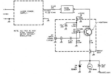
A current modulator is connected to the cathode of the laser. The quiescent current is set at 4.1 mA, and the modulating sigpal is set to vary the current only by ±0.7 mA. A well-protected and by-passed 0- to 10-mA meter is used in the ground leg to set and monitor the laser's quiescent operating current. A 51-kΩ, 2-W ballast resistor close to the anode lead of the laser stabilizes the discharge. The voltage across the sustaining supply should be 1.45 kV dc at full load. Remember that the subcarrier frequency must be no greater than 200 kHz, and that the peak-to-peak signal voltage into the modulator must not exceed 1.4 V p-p. (There are any number of ICs that operate as voltage controlled oscillators to produce the FM subcarrier.) (View)
View full Circuit Diagram | Comments | Reading(1521)
ABSOLUTE_VALUES
Published:2009/7/15 2:04:00 Author:Jessie
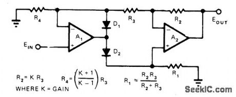
Positive output signal level is proportional to absolute value of input signal level, regardless of input polarity. Circuit combines simplicity with high input impedance, low output impedance, and greater than unity gain. Opamps A1 and A2 should have good CMRR and low offset and drift. D1 and D2 can be 1N914 For gain of 2.5, R1 and R3 are 1000 ohms, R2 is 2500, nd R4 is 2333 For unity gain, R4 is infinity and can be omitted R2 and R3 areequalue precision resistors Value of R1 is not critical at any gain.-R. Hofheimer, A Simple Absolute-Value Amplifier, EDN Magazine. June20, 1974, p 78 and 80. (View)
View full Circuit Diagram | Comments | Reading(1036)
LASER_MODULATION
Published:2009/7/14 11:51:00 Author:May

Electronic modulation of a laser beam can be handled in this fashion. Obviously, the transformer you use must be able to handle the high voltage from the laser power supply without breaking down. (View)
View full Circuit Diagram | Comments | Reading(1060)
LASER_RECEIVER_DETECTOR_AND_AUDIO_CIRCUIT_
Published:2009/7/14 11:49:00 Author:May

Video preamplifier output can be switched between an audio amplifier that establishes the correct level of the demodulated baseband audio when used for short distance test links and a phase-locked loop (PLL) that demodulates an FM subcarrier when used for longer distances. The PLL VCO is set to a 100-kHz subcarrier frequency. The error signal generated as the VCO tracks the FM signal produces the demodulated audio. Either of these outputs is sent to a 300- to 3000-Hz bandpass filter and on to an audio power amplifier capable of driving a low-impedance speaker or headphones. The dc power supply for these circuits is provided by a filtered 12 Vdc input. (View)
View full Circuit Diagram | Comments | Reading(2509)
SINGLE_HETEROSTRUCTURE_LASER_DRIVER
Published:2009/7/14 11:44:00 Author:May

One way to reliably achieve the fast rise-time pulse of short duration to power SH lasers is to use the phenomenon called avalanching of a transistor. Transistors have a breakdown voltage, abbreviated as Vceo; if this voltage is exceeded, the transistor will spontaneously conduct with its collectorto-emitter circuit open and the voltage applied to its collector. This produces a pulse whose rise time is extremely fast-on the order of 1 or 2 ns-and whose duration is related to the capacitance at the collector. The operation is as follows: Current rises at the base of transistor Q1 when the voltage on Cy has risen enough to jump over and break down the collector-to-emitter junction. For the 2N2222, this is typically 75 to 80 V. When the transistor breaks down, it sends a high-current pulse of energy through a low-value carbon film resistor R(s). With the 0.022-μF capacitor shown, the duration of the pulse to the laser is only about 75 ns. This capacitor must be specifically designed for low inductance. Note the high-speed switching diode D1. Its purpose is to damp out any reverse voltage that might occur in the circuit due to inductance after the laser turns off because a reverse voltage of only 3 V can destroy the SH laser. The rise time of this diode is comparable to that of the avalanche circuit, being only 6 ns before it begins to switch. The values of the capacitor and the current-limiting resistor R(s) depend upon the type of SH laser diode used. (View)
View full Circuit Diagram | Comments | Reading(998)
LOW_COST_LASER_DIODE_DRIVER
Published:2009/7/14 11:41:00 Author:May

The circuit presented is a low-cost laser-diode driver with current limiting and a lasing monitor for safe operation of the laser. The driver provides temperature stabilization using a built-in thermoelectric-cooler (TEC) controller. This circuit is designed around a QLM5S876 1.55-m laser-diode module with a built-in monitor photodiode, TEC, and thermistor. The laser is driven by the constant-current source Q2 and Q1. The drive current is stabilized against supply changes by Z1, limited by R2, and adjusted by R3 to the desired operating point. When the current is small, the laser doesn't lase and the monitor photodiode detects no optical power. As a result, comparator U1C goes below its trip point and LED1 turns off. When the current is adjusted and passes the laser threshold, sufficient optical power is generated by the laser, causing photo current to flow through the photodiode and the comparator to drive the lasing monitor indicator LED1 to on. The TEC controller circuit is a feedback system. If the temperature is higher than the set point, the comparator output will be high and will drive the TEC element through R15, Q3, and Q4. The TEC drive current is limited by Z2. When the TEC is driven on, it cools the laser. This increases the voltage of the inverting output until it passes the comparator's upper trip point and turns off the TEC's drive current. The temperature set point can be adjusted by R16. (View)
View full Circuit Diagram | Comments | Reading(6957)
INFRARED_DATA_RECEIVER
Published:2009/7/14 7:43:00 Author:May
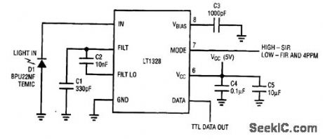
The LT1328 circuit operates over the full 1-cm to 1-m range of the IrDA standard at the stipulated light levels. For IrDA data rates of 115 kb/s and below, a 1.6-μs pulse width is used for a 0 and no pulse for a 1. Light levels are 40 to 500 mW/sr (milliwatts per steradian). The figure shows a scope photo for a transmitter input (top trace) and the LT1328 output (bottom trace). Note that the input to the transmitter is inverted; that is, transmitted light produces a high at the input, which results in a zero at the output of the transmitter. The MODE pin (pin 7) should be high for these data rates. (View)
View full Circuit Diagram | Comments | Reading(1186)
CASSETTE_RECORD_PLAYBACK
Published:2009/7/14 7:42:00 Author:May

National LM389 power amplifier chip includes three NPN transistors, to provide all circuits needed for complete recording and playback of cassette tapes. Two of internal transistors act as signal amplifiers while third is used for automatic level contra when recording. Diode is also on chip.- Audio Handbook, National Semiconductor, Santa Clara, CA, 1977, p 4-33-4-37. (View)
View full Circuit Diagram | Comments | Reading(1208)
IR_REMOTE_CONTROL_REPEATER
Published:2009/7/14 7:41:00 Author:May
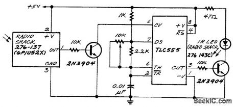
This circuit receives TV remote-control signals and retransmits them. The 555 oscillator provides 40-kHz modulation. The IR LED can be placed in another room. (View)
View full Circuit Diagram | Comments | Reading(793)
ULTRALOW_NOISE_PLAYBACK_PREAMP
Published:2009/7/14 7:39:00 Author:May

Provides optimum noise performance at popular tape speeds of 1 7/8 and 3 3/4 in/s. Reference gain for 0 dB is 41 dB, giving output level of 200 mV from head output of 1 mV at 1 kHz. Single-ended biasing and use of metal-film resistors reduce noise.- Audio Handbook, National Semiconductor, Santa Clara, CA, 1977, p 2-31-2-37. (View)
View full Circuit Diagram | Comments | Reading(822)
MONO_CORDLESS_HEADPHONE_IR_RECEIVER
Published:2009/7/14 7:37:00 Author:May
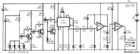
The full receiver circuit diagram appears in the figure. As many as four infrared detector can be used (D1 to D4 ). They are wired in parallel and used in the reverse-biased mode, and dark conditions only very small leakage currents flow. The pulses of infrared from the transmitter result in increased leakage currents, which generate small negative pulses at the cathodes (k) of the diodes. Transistor TR1 is used as a low-noise preamplifier and buffer stage. The majority of the voltage gain is provided by transistors TR2 and TR3, which are also common-emitter stages. These provide a combined voltage gain of over 80dB. The signal from TR3 is connected to one of the phase comparator inputs of IC1 (pin 14 ). This IC provides demodulation and is a CMOS 4046BE p.l.d. Resistor R10 and capacitor C6 are the timing components for the VCO,and they set the center frequency at approximately 100 kHz. Resistor R10 and capacitor C7 form a simple low-pass filter between the phase comparator’s output at pin 2 and the input of the VCO at pin 9. The audio output signal is obtained from the low-pass filter via an integral source-follower stage. The output from IC2 is fed to resistor R16 and capacitor C12, which form a simple low-pass filter that provides the deemphasis. The signal is then fed to the input of IC3, which is a small class-B audio power amplifier. The current consumption of the receiver is about 12 mA. (View)
View full Circuit Diagram | Comments | Reading(1693)
300_BAUD_BIT_BOFFER_RECEIVER
Published:2009/7/14 7:37:00 Author:May

Used with ordinary cassette recorder to convert half sine waves of recorded serial data to corresponding digital 1s and 0s. Output of recorder passes through filter and limiter IC6 to give square wave at point C whose zero crossings correspond to recorded sine wave. Leading and trailing edges of square wave are converted to narrow positive pulses by EXCLUSIVE-OR gate IC4 to give stream of pulses at D, one for each zero crossing. Transistor circuit forms retriggerable mono that is adjusted so point E goes positive three-fourths of way through low-frequency (1200 Hz) half-cycle. Point E then has stream of eight pulses for 0 and no pulses for 1. Final flip-flop provides recovery of data as is and 0s. Leading edge of waveform at D is shortened and combined with clock pulses to provide composite UART clock output. Boffer system eliminates errors commonly encountered when attempting to record square waves on tape with low-cost recorder.-D. Lancaster, TV Typewriter Cookbook, Howard VV. Sams, Indianapolis, IN, 1976, p 167-171. (View)
View full Circuit Diagram | Comments | Reading(1579)
PRECISION_SIGNAL_RECTIFIER
Published:2009/7/15 4:00:00 Author:Jessie

High input impedance at one of differential inputs of precision rectifier is achieved with opamp A1 whose output is switched between inputs of in-strumentation amplifier A2 by diodes. This switching reverses polarity of gain provided by A2, when signal polarity changes, so output signal is always positive.-J. Graeme, Measure Differential AC Signals Easily with Precision Rectifiers, EDN Magazine, Jan. 20, 1975, p 45-48. (View)
View full Circuit Diagram | Comments | Reading(802)
SYNCHRONOUS_VIDEO_DETECTOR
Published:2009/7/15 3:34:00 Author:Jessie

RCA CA3136E serves as video IF PLL synchronous detector for color TV receivers. Phase-locked oscillator demodulates 45.75-MHz video IF signals. Circuit features include automatic fine tuning voltage (AFT) for DC control of tuner, adjustment of zero-carrier DC level at video output terminal, amplifier arrangement for inverting noise impulses toward black level, and separate noninverting output terminal for sound IF. Re-quires single 12-V supply.- Linear Integrated Circuits and MOS/FET's, RCA Solid State Division, Somerville, NJ, 1977, p 374. (View)
View full Circuit Diagram | Comments | Reading(1773)
DELAYED_DROPOUT_RELAY_TIMER
Published:2009/7/15 3:25:00 Author:Jessie

Keeps relay energized for preset time of up to 10 sec after relay is pulled in by momentarily closing switch.- Transistor Manual, Seventh Edition, General Electric Co. 1964, p 324. (View)
View full Circuit Diagram | Comments | Reading(827)
10_RANGE_DC_VOLTMETER
Published:2009/7/15 3:25:00 Author:Jessie
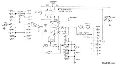
Rang switch is ganged between input and output circuits of CA3160 bipolar MOS opamp to permit selection of proper output voltage for feedback to terminal 2 of opamp through 10K current-limiting resistor. Circuit operates from single 8.4-V rnercury battery and draws about 500μA plus meter current;at input for full-scale reading, total supply current drain is about 1.5mA. –Circuit ldeas for PCA Liner ICs, RCA Solid State Division, Somerville, NJ, 1977, p 14. (View)
View full Circuit Diagram | Comments | Reading(1223)
SSTV_VERTICAL_SYNC_INDICATOR
Published:2009/7/15 3:24:00 Author:Jessie

Retriggerable mono MVBR using SN74123 is triggered by 0.125-Hz vertical sync pulse of amateur television system. Absence of pulse allows mono to time out and change state of LED from green to red. Vertical reset switch must then be used to p restart vertical sweep and reset LED. Uses Monsanto MV5491 dual red/green LED, with 220 ohms in upper lead to +5 V supply and 100 ohms in lower +5 V lead because red and green LEDs in parallel back-to-back have different voltage requirements. Drivers for LEDs are SN75454.-K. Powell, Novel Indicator Circuit, Ham Radio, April 1977, p 60-63. (View)
View full Circuit Diagram | Comments | Reading(1127)
| Pages:612/2234 At 20601602603604605606607608609610611612613614615616617618619620Under 20 |
Circuit Categories
power supply circuit
Amplifier Circuit
Basic Circuit
LED and Light Circuit
Sensor Circuit
Signal Processing
Electrical Equipment Circuit
Control Circuit
Remote Control Circuit
A/D-D/A Converter Circuit
Audio Circuit
Measuring and Test Circuit
Communication Circuit
Computer-Related Circuit
555 Circuit
Automotive Circuit
Repairing Circuit