
Circuit Diagram
Index 615
50_100_MC_PUSH_PUSH_DOUBLER
Published:2009/7/15 2:50:00 Author:Jessie
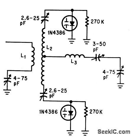
Charge-storage 1N4386 varactors in push-push provide 180 w. output with 70% effciency.-G.Schaffner, Charge Storage Varactors Boost Harmonic Power, Electronics, 3710, p 42-47. (View)
View full Circuit Diagram | Comments | Reading(747)
FIXED_MVBR_DELAY
Published:2009/7/15 2:50:00 Author:Jessie

Used to provide buffer interval between sync and video information in radar relay transmitter. Can be triggered by pulse. Accuracy of 30-microsec delay is only about 10%.-NBS; Handbook Preferred Circuits Navy Aeronautical Electronic Equipment, Vol. 1, Electron Tube Circuits, 1963, p N9-1. (View)
View full Circuit Diagram | Comments | Reading(564)
100_KC_TO_5_MC
Published:2009/7/15 2:49:00 Author:Jessie
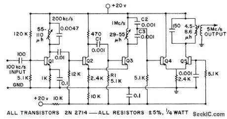
Simple transistor circuit converts 100-kc standard frequency of frequency counter to 5 Mc for use with 500-Mc frequency converter which requires 5.Mc reference frequency. Q1 is doubler. Q2 and Q3 form unique quintupler evolved from Schmitt trigger, in which square-wave symmetry is preserved by maintaining triggering point at zero crossings of input signal. Q4-05 is similar quintupler, but without cross-coupling feedback.-H. T. McAleer, Unique Frequency Multiplier, Frequency, May-June 1964, p 36-37. (View)
View full Circuit Diagram | Comments | Reading(788)
INPUT_INVERTING_DELAY
Published:2009/7/15 2:49:00 Author:Jessie

Input voltage, supply voltage EBB, and R1.C1 determine delay time for digital pulses.-R.A. Karlin, One-Transistor Multi Delays Digital Pulses, Electronics, 38:17, p 85-86. (View)
View full Circuit Diagram | Comments | Reading(627)
IR_REMOTE_CONTROL_RECEIVER
Published:2009/7/14 8:16:00 Author:May
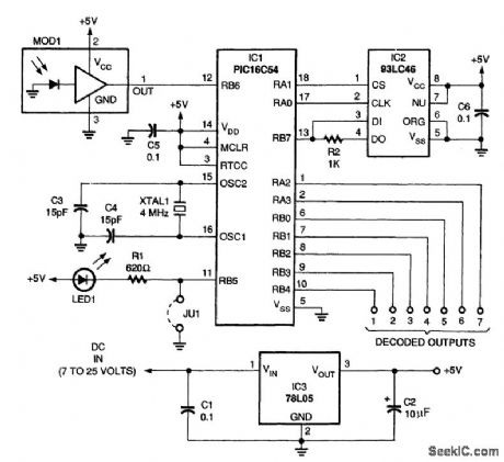
A schematic diagram of the remote-control receiver is shown. The heart of the circuit is IC1, a PIC16C54 8-bit CMOS manufactured by Microchip. The microcontroller stores its data in IC2, a 93LC46 1-kbit serial EEPROM (electrically erasable programmable read-only ntemory), also manufactured by Microchip. In this application, the 93LC46 has a three-line interface with the microcontroller. The three lines are CHIP SELECT, CLOCK, and DATA IN/OUT. Because DATA IN and DATA OUT share the same line, a resistor (R2)limits the current flow during transitions between writing and reading when there are conflicting logic levels. The microcontroller communicates with the 93LC46 by placing a logic high on the CHIP SELECT pin. Data are then transferred serially to and from the 93LC46 on the positive transition of the CLOCK line. Each read or write function is preceded by a start bit, an opcode identifying the function to be performed (read, write, etc.), then a 7-bit address; this is followed by the 8 bits of data which are being written to or read from that address. Immediately preceding and following all write operations, the microcontroller sends instructions to the 93LC46, which enables or disables the write function, thereby protecting the data that have been stored. In the programming mode, IC1 reads an IR data stream from MOD1 and converts it to data patterns that can be stored in IC2. These data patterns are held for comparison while the unit is in normal operation. Power for the circuit is conditioned by IC3, a 78L05 low-current, 5-V regulator, which will accept any dc input voltage between 7 and 25 V. Capacitors C1 and C2 stabilize the operation of the regulator. Crystal XTAL1 sets the internal oscillator of IC1 to 4 MHz. Jumper JU1 consists of two closely spaced pads on the PC board that, when momentarily jumpered with a screwdriver or other piece of metal, places IC1 in the programming mode and lights LED1. The source and object code are available on the Gernsback BBS (516-293-2283, v.32, v.42bis) as a file called IREC.ZIP for those who wish to program their own PICs and have the proper equipment to do so. (View)
View full Circuit Diagram | Comments | Reading(5300)
SLOW_BREAK_RELAY
Published:2009/7/15 2:48:00 Author:Jessie

R3-C1 determine period that relay remains energized after input pulse is removed.-P. Haas, Timing Circuits Control Relays, Electronics, 38:6, p 85. (View)
View full Circuit Diagram | Comments | Reading(552)
CASCADED__UHF_DOUBLERS
Published:2009/7/15 2:47:00 Author:Jessie
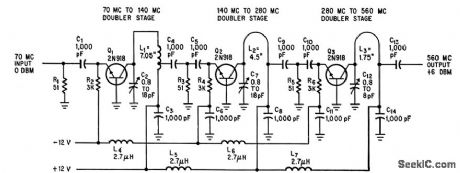
Common-base amplifier with tank circuit tuned to twice the input frequency is cascaded to give frequency multiplication in 40 to 1,000 Mc range, with power output per stage ranging from 50% of stage d-c supply at low frequencies to 25% at high frequencies.-A. E. Munich, Basic UHF Circuit Forms Amplifiers and Multipliers, Electronics, 37:20, p 59-60. (View)
View full Circuit Diagram | Comments | Reading(784)
IR_LOCAL_TALK_LINK_RECEIVER
Published:2009/7/14 8:13:00 Author:May


A low-noise (2 pA /√Hz),high-bandwidth (7 MHz) current-to-voltage converter formed by the preamplifier and its associated components transforms the reverse current from an external photodiode to a voltage. Although the 7-MHz bandwidth of the prearnp supports 4-Mbit data rates, a low-pass filter on the preamp output is used to reduce the bandwidth to just the required amount in order to reduce noise. As shown, capacitance CF1 sets the break frequency of an ac high-pass loop around the preamp to 180 kHz. This loop rejects unwanted ambient light, including sunlight and light from incandescent and fluorescent lamps. The preamp stage is followed by two separate channels, each containing a high-impedance filter buffer, two gain stages, high-pass loops, and a comparator. The only difference between the two channels is the response time of the comparators: 25 and 60 ns. For the 125-ns pulses of IR LocalTalk, the 25-ns comparator with its active pull-up output is used. The low-frequency comparator with its open collector output (with 5 kΩ internal pull-up) is suitable for more modest speeds, such as the 1.6-ps pulses or the IrDA-SIR. Each gain path has an ac coupling loop similar to the one on the preamp. Capacitance CF5 sets the high-pass comer at 140 kHz for IR LocalTalk. The loops serve the additional purpose here of maintaining an accurate threshold for the comparators by forcing the dc level of the differential gain stages to zero. As the preamp output is brought out and the inputs to the two comparator channels are buffered, the user is free to construct the exact filter required for the application by the careful selection of external components. RF1,CF2,CF3,RF4,CF4, and RF3 form a bandpass filter with a center frequency of 3.5 MHz and 3-dB points of 1 MHz and 12 MHz. Together with the high-pass ac loop in the preamp and the 7-MHz response of the preamp, this forms an optimal filter response for IR LocalTalk.
(View)
View full Circuit Diagram | Comments | Reading(714)
45_W_SERIES_TYPE_POWER_AMPLIFIER
Published:2009/7/15 2:47:00 Author:Jessie

Uses split-load phase inverter, capacitance-coupled to common-collector class B driver,which in turn is direct-coupled to class-B common-emitter output stage. Driver and output stages are each in series for d-c collector supply. No transformers are required.-M. B.Herscher, Designing Transistor A-F Power Amplifiers, Electronics, 31:15, p 96-99. (View)
View full Circuit Diagram | Comments | Reading(983)
TWO_DOUBIERS_AND_QUADRUPLER_GIVE_960_MC
Published:2009/7/15 2:46:00 Author:Jessie
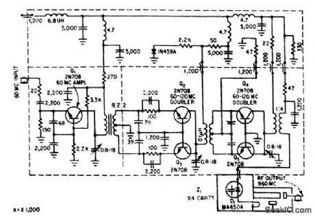
First two doublers are push-push class C with unity gain. Varactor D1 in final multiplier, feeding 960.Mc quarter-wave series-resonance coaxial cavity, acts as quadrupler.-W. E. Dahl, Communicating with Future Deep-Space Probes, Electronics, 36:22, p 28-32, (View)
View full Circuit Diagram | Comments | Reading(667)
PHONE_CALL_COUNTER
Published:2009/7/14 8:12:00 Author:May

Circuit actuates solenoid that depresses R/S counting key of SR-56 calculator for each interrogation event consisting of sequence of pulse bursts each corresponding to ring of phone. Bursts are separated by 4-s pauses, so circuit includes time delay that prevents actuation of solenoid until line has remained quiescent for more than 5 s after burst. Article includes program that is inserted in calculator to total number of times R/S key is de-pressed. Applications include counting number of telephone calls received while away.-M. Bram, Hardware + Program Makes SR-56 Event Counter, EDN Magazine, Aug. 5, 1978, p 84 and 86. (View)
View full Circuit Diagram | Comments | Reading(0)
SINGLE_TONE_DECODER
Published:2009/7/14 8:11:00 Author:May

Used at receiving end of leased telephone line in which single tone frequency serves for alarm and other purposes. A1 is 741 opamp connected as inverting amplifier, with R1 and R3 chosen to match input impedance and R2 chosen to give gain required for available input signal level. For 10K input impedance, R1 and R3 are 10K and R2 in kilohms is 10 times required gain (500K for gain of 50). Actual tone decoding is performed by A2, which is also 741; here C3, C4, R8, and R9 are frequency-determining components and R6 is gain control. R4 is chosen to give desired bandwidth ; use 470K for 5-10%, 1 meg ohm for 3-5%, and 2.2 meg ohms for 1-3%. R8 is same as R2, and R9 equals R3. Diodes are 1N914.-C. D. Rakes, Integrated Circuit Projects, Howard W. Sams, Indianapolis, IN, 1975, p 60-66. (View)
View full Circuit Diagram | Comments | Reading(896)
FM_FOR_INSTRUMENTATION
Published:2009/7/14 8:07:00 Author:May

Frequency modulator-demodulator circuit using IC and opamp converts ordinary low-cost tape recorder into instrumentation recorder. Signetics NE565 phase-locked loop serves for both modulation and demodulation. Frequency response of 0-800 Hz is suitable for recording VLF phenomena at tape speed of 9.1 cm/s (3.5 in/s). Carrier frequency is in midband, at 3 kHz. Article covers circuit operation in detail and gives de-sign equations.-B. D, Jordan. Simple F.M.Modulator/Demodulator for a Magnetic Tape Recorder, Wireless World, March 1974, p 29-30. (View)
View full Circuit Diagram | Comments | Reading(3900)
FSK_DETECTOR_FOR_CASSETTE_RECORDED_DATA
Published:2009/7/14 8:05:00 Author:May

Connection shown for 565 PLL provides data output of 1 for 6.4 kHz and 0 for 4.8 kHz from ordinary cassette tape recorder having frequency response to 7 kHz. Report gives circuit of suitable recorder using return-to-zero FSK. System also requires 800-Hz clock generator for synchronizing to data. Up to seven 0s can occur in succession without making clock go out of sync. Odd parity is used.- Signetics Analog Data Manual, Signetics, Sunnyvale, CA, 1977, p 857-859. (View)
View full Circuit Diagram | Comments | Reading(1843)
CASSETTE_DATA_PLAYBACK
Published:2009/7/14 8:02:00 Author:May

Converts low-level digital signals from cassette recorder into CMOS-compatible 5-V square waves. Both in-puts of 3130 opamp are biased to +2 V for use as open-loop comparator. RC input filter minimizes hum and bias interference.-D. Lancaster, CMOS Cookbook, Howard W. Sams, Indianapolis, IN, 1977, p 345. (View)
View full Circuit Diagram | Comments | Reading(648)
ISOLATING_DIODE_MONO_MVBR
Published:2009/7/15 2:46:00 Author:Jessie

Addition of diode D1 to conventional delay circuit reduces timing variations otherwise encountered in production runs. Supply voltage change of 10% causes timing change of only 1%-D. E. Haselwood. Monostable Multivibrators with Stable Delay Times. Electronics.34:49,p64-65 (View)
View full Circuit Diagram | Comments | Reading(563)
NAB_TAPE_PREAMP
Published:2009/7/14 8:01:00 Author:May

One section of Signetics NE542 dual noise amplifier is used to provide 100-mV output level at 1 kHz following NAB equalization curve for tape speed of 7 1/2 in/s.- Signetics Analog Data Manual, Signetics, Sunnyvale, CA, 1977, p 780. (View)
View full Circuit Diagram | Comments | Reading(1840)
500_MEG_D_C_INPUT_RESISTANCE
Published:2009/7/15 2:45:00 Author:Jessie
Bootstrap-collector circuit uses starved transistor to provide 500-meg d-c input resistance with 100-v input signal. A-c resistance is even higher, in the 1,000-megohm region at low audio frequencies.-B. M.Bramson, Starved Transistors Raise D-C Input Resistance, Electronics, 32:5, p 54-55. (View)
View full Circuit Diagram | Comments | Reading(934)
AVC_AND_VOX
Published:2009/7/14 7:59:00 Author:May

Voice-operated ON/OFF switch uses microphone to sense normal back-ground sound. Anything above background threshold preset by R16 energizes relay K for turning on recorder. Circuit provides about 2-s delay after subject stops talking, before releasing relay. Automatic volume control circuit keeps recorded signal essentially constant despite movements of loudspeaker toward or away from microphone.-G. Beard, Automatic Volume and VOX for Your Tape Recorder, Popular Science, Oct. 1973, p 134 and 136. (View)
View full Circuit Diagram | Comments | Reading(1341)
TWO_54_MC_OUTPUTS_FROM_3_MC
Published:2009/7/15 2:45:00 Author:Jessie

Uses three class AB common-emitter amplifiers.First two are triplets that multiply 3-Mc input to 27 Mc. Third doubles this to 54 Mc, and drives two parallel 54.Mc class AB output amplifiers providing 25 mw each.-J. W. Hamblen and J. B. Oakes, Instrumentation and Telemetry of Transit Navigational Satellites, Electronics, 34:32, p 148-153. (View)
View full Circuit Diagram | Comments | Reading(662)
| Pages:615/2234 At 20601602603604605606607608609610611612613614615616617618619620Under 20 |
Circuit Categories
power supply circuit
Amplifier Circuit
Basic Circuit
LED and Light Circuit
Sensor Circuit
Signal Processing
Electrical Equipment Circuit
Control Circuit
Remote Control Circuit
A/D-D/A Converter Circuit
Audio Circuit
Measuring and Test Circuit
Communication Circuit
Computer-Related Circuit
555 Circuit
Automotive Circuit
Repairing Circuit