
Circuit Diagram
Index 618
STABLE_ENCODER
Published:2009/7/14 6:15:00 Author:May

All tones are frequency-synthesized and held within tolerance of 0.2% by using Motorola MC14410P CMOS tone-en-coder chip which is digital synthesizer requiring only 1-MHz reference crystal and nine other external parts. Circuit is redesign of Heath Mi-coder for triggering autopatch of repeater during mobile operation. Operates from 9-V battery. Audio output matches input for low-impedance microphone. For higher output, increase R3 and R4.-G. K. Fallenbeck, Mycoder, QST, April 1978, p 27-29. (View)
View full Circuit Diagram | Comments | Reading(794)
30_4000_Hz_WITH_OPAMP
Published:2009/7/15 2:35:00 Author:Jessie
Frequency is determined by pot R1 in feedback path. Square-wave output pulse amplitude is about 5 V. Circuit will generate almost perfect sine waves if 0.1-μF capacitor is connected between pin 12 and ground; R1 must be properly adjusted to give output of about 220 Hz. - F. M. Mims,″Integrated Circuit Projects, Vol. 6,″Radio Shack, Fort Worth,TX,1977, p 89-95. (View)
View full Circuit Diagram | Comments | Reading(775)
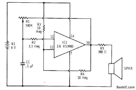
BASS_BOOST_OR_LOUDNESS_CONTROL
Published:2009/7/15 2:35:00 Author:Jessie

Operates on output of preamp.Gives operator independent control of level of bass or amount of bass boost desired. May also be used as loudness control.- Transistor Manual, Seventh Edition, General Electric co.,1964,p 254. (View)
View full Circuit Diagram | Comments | Reading(3692)
DARLINGTON_AMPLIFIER
Published:2009/7/15 2:34:00 Author:Jessie

Useful up to 100 kc, but high input impedance makes it particularly desirable for audio preamps. Gives gain of two stages with dissipation of only one.-L. Pollock and R. Gutteridge, Latest Design Techniques for Linear Microcircuits, Electronics, 35:41, p 47-49. (View)
View full Circuit Diagram | Comments | Reading(1121)
FOUR_MINUTE_DELAY
Published:2009/7/15 2:34:00 Author:Jessie

Ujt switch gives accuracy of 1% for time delays in range of 1 to 4 minutes, over range of 10℃ above and below 25℃. R1 controls amount of delay.-E. G. McCoy, Accurate Time Delays up to Four Minutes, EEE, 11:10, p 31. (View)
View full Circuit Diagram | Comments | Reading(673)
DC_VOLTMETER
Published:2009/7/15 2:33:00 Author:Jessie

Opamp connected for closed-loop gain of 100 is used with attenuator network and 100-μA microammeter to serve as general-purpose multirange laboratory voltmeter. Additional full-scale output of ±10 V is provided for driving chart recorder. Low-pass filter R4-R5-C1-C2 prevents amplifier from overloading on large AC input signals while allowing circuit to read DG component. Filter acting with diodes protects amplifier from input overloads up to1000 V.-R. S, Burwen, Simple DC Voltmeter Uses Single Op Amp, EDN/EEE Magazine, Dee. 15, 1971, p 57. (View)
View full Circuit Diagram | Comments | Reading(0)
INFRARED_ALARM_RECEIVER
Published:2009/7/14 7:33:00 Author:May
The full circuit diagram for the infrared receiver is given here. TR1 is a phototransistor, and it is used in a common-emitter amplifier. However, no bias current is fed to the base (b) terrrtinal of TR1.The collector (c) current is governed by the light level received by TR1. The higher the received light level, the higher the current flow. The pulses of infrared from the transmitter therefore produce pulses of leakage current through TR1, which give small negative pulses at TR1's collector. The output signal for TR1's collector is coupled by capacitor C2 to a high-gain inverting amplifier based on IC1. Resistors R2 and R5 ire the negative-feedback network, and these set the closed-loop voltage gain of IC1 at 220 times. Capacitor C4 couples the amplified output signal from IC1 pin 6 to a conventional half-wave rectifier and smoothing circuit (D1, D2, and C5). Germanium, rather than silicon, diodes are used in the rectifier, because germanium types have a lower forward voltage drop.This gives slightly improved sensitivity. The positive dc signal developed across capacitor C5 drives the base of TR2, which is a simple common-emitter switch that controls the relay RLA coil. (View)
View full Circuit Diagram | Comments | Reading(2645)
20_W_60_CPS_INVERTER
Published:2009/7/15 2:33:00 Author:Jessie

Low-power version was designed to drive timer. Maximum frequency variation was only 1 % for supply-voltage range of 11.5 to 14.5 v.-Texas lnstruments lnc,, Transistor Circuit Design, McGrctw4iill, N.Y., 1963,p458. (View)
View full Circuit Diagram | Comments | Reading(795)
CASSETTE_INTERFACE_WITH_ACIA
Published:2009/7/14 7:31:00 Author:May

Permits use of audio pickup for mass storage in Motorola 6800 microcomputer system. Uses Motorola MC6850 asynchronous communication interface adapter (ACIA), which is specialized version of UART. All control, status, and data transfers in ACIA are made over single 8-bit bidirectional bus. Request-to-send line (RTS) controls tape recorder motor. When RTS is set high, input to IC8 is high and relay coil is not energized. IC6 gives 5-s delay following motor turn-on so long leader will be recorded at mark frequency. IC7 gives delay so reading starts 2.5 s before first data byte. Article covers circuit operation in detail and gives operating subroutines.-J. Hemenway. The Compleat Tape Cassette Interface, BYTE, March 1976, p 10-16. (View)
View full Circuit Diagram | Comments | Reading(3164)
VARIABLE_FREQUENCY_UP_TO_05_MHz
Published:2009/7/15 2:33:00 Author:Jessie


Frequency is determined by choice of values for C and frequency-control potentiometer R4.Square-wave output has almost equal mark-space ratio over wide frequency range. Regenerative action is rapid, reducing transition times. When circuit is switched on, C is uncharged and Tr2 is on. C charges until Tr1 begins to conduct, cutting off Tr2 and discharging C through R4 until Tr1 cuts off and cycle repeats.-J.L. Linsley Hood, Square-Wave Generator with Single Frequency-Adjustment Resistor, Wireless World, July 1976, p 36.
(View)
View full Circuit Diagram | Comments | Reading(848)
MONO_CORDLESS_HEADPHONE_IR_TRANSMITTER
Published:2009/7/14 7:30:00 Author:May
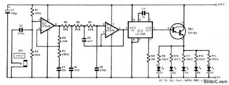
The preemphasis is applied by IC1, which is basically just an op amp used in the noninverting mode. At low and middle frequencies, the impedance of capacitor C3 is high in relation to the resistance of R3. Consequently, there is virtually 100 percent negative feedback through resistor R3, and IC1 has a closed-loop gain of little more than unity. At higher frequencies, the impedance of C3 is relatively low, and a significant proportion of the feedback through R3 is decoupled. This gives a closed-loop voltage gain that steadily rises with increased input frequency, with almost 20 dB of gain being provided at the highest audio frequencies. Resistor R4 limits the closed-loop voltage gain of IC1 at frequencies above the audio range. The low-pass filter is a conventional third-order (18 dB/octave) type based on IC2. This filter gives fractionally less than the full 20-kHz audio bandwidth, but does not significantly impair the quality of the input signal. A CMOS “micropower” PLL is used for IC3, but, in this circuit, only the VCO stage is utilized. No connections are made to any of the other sections of IC3. The output of IC2 is direct-coupled to the control input of the VCO (IC3 pin 9). Capacitor C7 and resistor R8 are the VCO timing components, and they set the center frequency at roughly 100 kHz. Transistor TR1 is a high-gain power Darlington device, which is used here as an emitter-follower buffer stage. This can easily source the 500-mA ON current of the LEDs. A bank of five LEDs is used, and each one has a separate current-limiting resistor (R9 to R13). (View)
View full Circuit Diagram | Comments | Reading(1655)
MODIFIED_PHANTASTRON_INTEGRATOR
Published:2009/7/15 2:31:00 Author:Jessie

Addition of input emitter-follower Q1 increases open-loop current gain of integrator and provides increased accuracy and linearity.-S. R. Parris and D. A, Staar, Highly Accurate Phantastron Delay Circuit, Electronics, 33:43, p 72-74. (View)
View full Circuit Diagram | Comments | Reading(681)
25_W_CLASS_B_POWER_AMPLIFIER
Published:2009/7/15 2:31:00 Author:Jessie
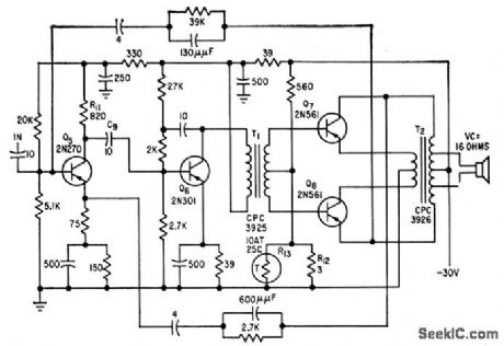
Uses balanced negative feedback, with input Q5 and driver Q6 operating class A.Output stage is temperature-stabilized.-R. Minton, Designing High-Quality A-F Transistor Amplifiers, Electronics, 32:24, p 60-61. (View)
View full Circuit Diagram | Comments | Reading(982)
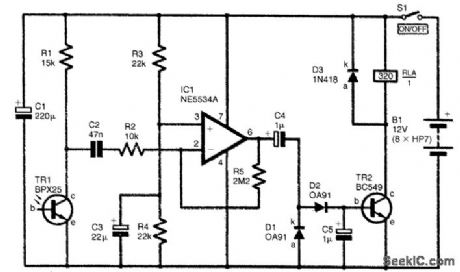
INFRARED_ALARM_TRANSMITTER
Published:2009/7/14 7:28:00 Author:May

The circuit diagram for the infrared transmitter appears in this figure. The oscillator uses IC1 as a relaxation oscillator. Capacitor C2 and resistor R4 are the timing components, and they are connected between the output of IC1 and its inverting input (pin 2). A roughly square-wave signal is generated at pin 6, the output of IC1. This signal is used to drive infrared LED D1, via emitter-follower buffer-stage transistor TR1 and current-limiter resistor R5. The specified value for R5 sets the LED current at nearly 100 mA, but as the LED is switched off for about 50 percent of the time, the average LED current is a little under 50 mA. This is the maximum acceptable drive current for most normal infrared LEDs. (View)
View full Circuit Diagram | Comments | Reading(1409)
FAST_RECHARGING_PHANTASTRON
Published:2009/7/15 2:30:00 Author:Jessie

Recharging of solid-state phantastron delay capacitor is reduced to 5microsec by addition of Q7. Circuit of Q7 is inoperative during all other parts of cycle, including quiescent state.-S. R. Parris and D. A Staar, Highly Accurate Phantastron Delay Circuit, Electronics, 33:43, p 72-74. (View)
View full Circuit Diagram | Comments | Reading(779)
50_DUTY_CYCLE_WITH_555
Published:2009/7/15 2:30:00 Author:Jessie
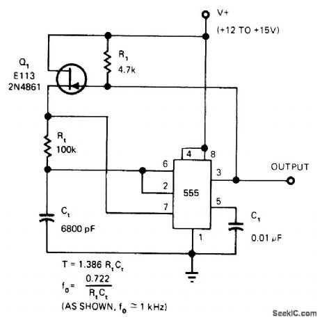
Provides pure square-wave output without sacrificing allowable range of timing resistance. Q1 replaces conventional timing resistor going to V+. Pull-up resistor R1 is required to switch Q1 fully on when it is driven by output of timer.-W. G. Jung, Take a Fresh Look at New IC Timer Applications, EDN Magazine, March 20, 1977, p 127-135. (View)
View full Circuit Diagram | Comments | Reading(1281)
FOUR_SPEED_PLAYBACK_PREAMP
Published:2009/7/14 7:28:00 Author:May
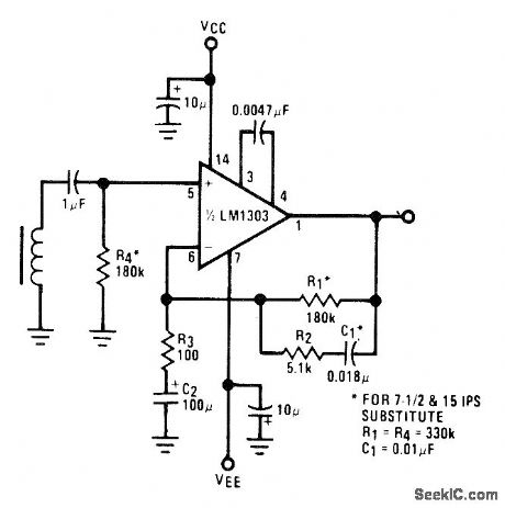
Provides 0-dB reference gain of 34 dB. Supply can be ±4.5 to ±15 V. Values shown are for NAB equalization and 1 7/8 or 3 3/4 in/s; for 7 1/2 and 15 in/s, change values as indicated. Design equations are given.- Audio Handbook, National Semiconductor, Santa Clara, CA, 1977, p 2-31-2-37. (View)
View full Circuit Diagram | Comments | Reading(1066)
LOW_COST_IR_FILTER
Published:2009/7/14 7:26:00 Author:May

When exposed to “cool white” fluorescent light for 5 s, the color negative (using Kodacolor 100 ASA film) produced after the developing process exhibits a sharp cutoff at about 830 mm. This is perfect for many IR LEDs and other IR devices. (View)
View full Circuit Diagram | Comments | Reading(823)
IR_REMOTE_TESTER
Published:2009/7/14 7:25:00 Author:May

This remote handset tester is very useful and convenient, and could quickly pay for itself by helping to recover faulty remote handsets. Pulsed infrared light generated by the handset falls upon D1, which creates a pulse waveform across R1. This is capacitively coupled to the base of TR1, and an amplified signal is coupled to C2 to a pulse-stretching circuit based around TR2, C3, and associated components. Hence, driver transistor TR3 conducts and illuminates the LED D2 whenever infrared light is received by D1. A functional remote controller with fresh batteries will operate the tester from approximately 500 mm, while one with nearly exhausted batteries may work over only a few centimeters. Coincidentally, the design also self-tests its own battery by giving an initial flash of D1 when the switch S1 is first closed. The IR photodiode should be roughly a 940-nm type, while the types of the transistors themselves are not crucial. The circuit will operate from a 6- to 12-V rail (e.g., a 12-V battery), and C4 decouples the power supply rails. (View)
View full Circuit Diagram | Comments | Reading(1105)
WARBLE_TONE_INFRARED_TRANSMITTER
Published:2009/7/14 7:23:00 Author:May
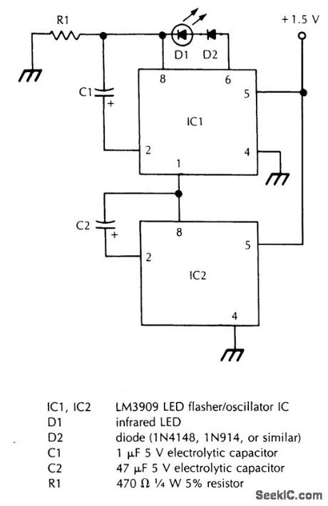
IC1 and IC2 are LM3909 LED flasher-oscillator devices. IC2 generates a low-frequency square wave that modulates the frequency of IC1. This circuit is useful for IR testing, communications link signal source, etc. (View)
View full Circuit Diagram | Comments | Reading(997)
| Pages:618/2234 At 20601602603604605606607608609610611612613614615616617618619620Under 20 |
Circuit Categories
power supply circuit
Amplifier Circuit
Basic Circuit
LED and Light Circuit
Sensor Circuit
Signal Processing
Electrical Equipment Circuit
Control Circuit
Remote Control Circuit
A/D-D/A Converter Circuit
Audio Circuit
Measuring and Test Circuit
Communication Circuit
Computer-Related Circuit
555 Circuit
Automotive Circuit
Repairing Circuit