
Circuit Diagram
Index 617
50_MC_TO_400_MC_VARACTOR_MULTIPLIER
Published:2009/7/15 2:40:00 Author:Jessie

Consists of two push-push varactor circuits in cascade, with bandpass filter at output.Provides 40 w with 30% conversion efficiency; For pulse-modulated drive signals, will give 100 w peak pulse power at 0.0088 duty cycle. Uses Motorola 1N4386 varactors. -J. Cochran, Two-State Varactor Multiplier Provides High Power at 400 Mc, motorola Application Note AN-177, Aug. 1965. (View)
View full Circuit Diagram | Comments | Reading(802)
SWEEP_GENERATOR
Published:2009/7/14 7:09:00 Author:May


Both IC2 and IC4 are Exar XR2206 monolithic function generators; IC4 functions as a ramp generator, and IC2 functions as a generator of sine, triangular, and square waveforms. Dual operational-amplifier IC1 produces a scaled, level-shifted ramp output that is capable of deflecting an oscilloscope's horizontal sweep. This ensures that the sweep generator and the oscilloscope's sweep circuit are always properly synchronized. Any frequency of interest along the horizontal axis of an oscilloscope that is coupled to this function generator can be measured with an extemal frequency counter by manually tuning the function generator's VCO instead of sweeping it. The performance characteristics of the sweep/function generator are summarized in Table 1. The generator's sweep rate and frequency can be set by front-panel rotary six-position switches, SWEEP RATE switch S5 and FREQUENCY switch S2. The VCO control R30 manually tunes the VCO. Table 2 lists the sweep ranges of the function generator. Sweep ranges other than those covered in ranges 1 to 4 can be set up as required on positions 5 and 6. Selecting the VCO setting on the front-panel toggle switch S4 permits tuning any fixed frequency within the total frequency range of the instrument with both the FREQUENCY switch S2 and VCO control R30.
(View)
View full Circuit Diagram | Comments | Reading(0)
MULTIPLIER_GIVES_324_MC
Published:2009/7/15 2:39:00 Author:Jessie
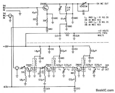
Two class B common-base stages (one tripler and one doubler) drive class AB common-base output amplifier to give 50 mw at 324 Mc from 54-Mc input. Upper section, a 54-Mc transmitter, is simply a single class AB common emitter that gives 200 mw output from 25-mw input.-J. W. Hamblen and J. B. Oakes, Instrumentation and Telemetry of Transit Navigational Satellites, Electronics, 34:32, p 148-153. (View)
View full Circuit Diagram | Comments | Reading(619)
ULTRA_FAST_MONOCYCLE_GENERATOR_
Published:2009/7/14 7:03:00 Author:May
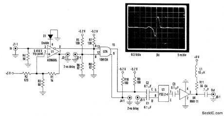
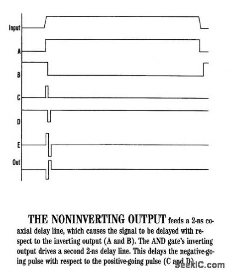
This circuit (Fig. 1a) can test an ultra-fast sample-and-hold amplifier, producing the monocycle shown (Fig.1b) when triggered with a TTL input pulse. The comparator (U1) squares up the input pulse and drives the AND gate (U2) with complementary outputs. The hysteresis resistors are chosen to provide reliable triggering despite the 50-Ω loading of the TTL input. The noninverting comparator output feeds a 2-ns coaxial delay line, causing the signal to be delayed with respect to the inverting output (Fig. 2). This forces the outputs of the AND gate to change state for a period of time equal to the delay. The inverting output of the AND gate drives a second 2-ns delay line, delaying the negative-going pulse, with respect to the positive-going pulse (Fig. 2). The power combiner (U3) sums the signals, producing a monocycle output. U4 amplifies the signal. Shorter pulses could be produced by shortening the delay lines and replacing U2 with an AND gate from a faster ECL family. (View)
View full Circuit Diagram | Comments | Reading(1527)
2_10V_P_P_TRUE_RMS_T0_600_kHz
Published:2009/7/15 2:38:00 Author:Jessie

Input waveform is squared by first Motorola MC1594 multiplier, and current output is converted to voltage by opamp for driving second multiplier which has capacitor in feedback path to perform averaging function. Second opamp is used with second multiplier as feedback element to produce square-root configuration required for giving true RMS value. Accuracy is within 1% over input voltage range.-K. Huehne and D. Aldridge, Multiplier/Op Amp Circuit Detects True RMS, Motorola, Phoenix, AZ, 1974, EB-20.
(View)
View full Circuit Diagram | Comments | Reading(980)
SIMPLE_FREQUENCY_GENERATOR_
Published:2009/7/14 7:00:00 Author:May


The circuit diagram for a simple frequency generator that uses a divide-by-N counter, based on a single 74HC161, is shown. Although IC1a and IC1b are NOR gates, in this circuit, they are used as inverters in a crystal clock generator. This provides an accurate 2-MHz output signal that is fed to the input of the divide-by-N circuit based on IC2 and IC1c. An inversion is needed between the comparator output and the negative active preset enable input, and this inversion is provided by IClc.Unfortunately, setting the division rate is more convoluted than simply writing the required value for N to the data inputs (D0 to D3). Table 1 shows the division rates and output frequencies for the 16 input codes for IC2. If the data inputs of IC2 are controlled via inverters, the division rate is one more than the value written to the port. Without a hardware inversion, a software inversion is required.This is actually quite easy, and it is just a matter of deducting the required division rate from 16 (e.g., for a division rate of 4, a value of 12 is written to IC2). Notice that the minimum division rate is 2, and that writing a value of 15 to IC2 will not give a division by 1. (View)
View full Circuit Diagram | Comments | Reading(2737)
DOUBLERS_AND_TRIPLER
Published:2009/7/15 2:38:00 Author:Jessie

In left section, first two stages are class B common-base power doublers and last two AB common-emitter amplifiers. Output is 150 mw at 216 Mc input. In section at right, common-base class B power tripler drives common-emitter output amplifier to give 140 mw output at 162 Mc from 54-Mc input.-J.W. Hamblen and J. B. Oakes, Instrumentation and Telemetry of Transit Navigational Satellites,Electronics,34:32, p 148-153. (View)
View full Circuit Diagram | Comments | Reading(597)
300_BAUD_BIT_BOFFER_TRANSMITTER
Published:2009/7/14 6:54:00 Author:May

Permits recording of serial data on ordinary Iow-cost cassette tape recorders for bulk storage of data to be used later in microprocessor. Requires 19,200-Hz reference input to terminal XC from external clock. Feedback from sine-wave synthesizer IC1 to dividby-4 counter IC2 automatically synchronizes system so sine waves automatically switch just before zero crossing each time serial data changes from 1 to 0 or back again. Output consists of 16 half sine waves at 2400 Hz for mark or digital 1 and 8 half sine waves at 1200 Hz for space or digital 0, for feed to input of cassette recorder. Circuit eliminates errors commonly encountered when attempting to record square waves on tape with low-cost recorder.-D. Lancaster, TV Typewriter Cookbook, Howard W. Sams, Indianapolis, IN, 1976, p 167-171. (View)
View full Circuit Diagram | Comments | Reading(1950)
FIXED_BOOTSTRAP_DELAY
Published:2009/7/15 2:37:00 Author:Jessie

Used to provide buffer interval between sync and video information in radar relay transmitter. Requires gate at least as long as 30-microsec delay. Accuracy is only 10%.-NBS, Hand-book Preferred Circuits Navy Aeronautical Electronic Equipment, Vol.1, Electron Tube Circuits, 1963, p N9-1. (View)
View full Circuit Diagram | Comments | Reading(536)
150_450_MC_TRIPLER
Published:2009/7/15 2:37:00 Author:Jessie

Charge-storage 1N4387 varactor gives 20 w at 450 Mc of 150-Mc input.-G. Schaffner, Charge Strorage Varactors Boost Power,Electronics,37:20, p42-47. (View)
View full Circuit Diagram | Comments | Reading(734)
IC_MILLIVOLTMETER
Published:2009/7/15 2:36:00 Author:Jessie


Provides switched ranges of 5 mV to 500 V. Use 2% resistors. Pushbutton connection to positive supply gives internal calibration check on 5-V and 50-V ranges. Adjust meter initially with Rm, to read 1.4 V on 5-V range. Back-to-back signal diodes provide overload protection. Power drain is so low that battery life is essentially shelf life.-D. A. Bundey, Where is Your Simplified, Sensitive, Milli-voltmeter?, 73Magazine, Sept. 1975, p 49-50. (View)
View full Circuit Diagram | Comments | Reading(957)
DUAL_TONE_SIGNALING
Published:2009/7/14 6:51:00 Author:May

American Microsystems S2559 digital tone generator IC at upper right interfaces directly with encapsulated 500-type telephone set to give pushbutton dualtone telephone. Diodes D1-D4 are added to telephone set to ensure that polarity of direct voltage across device is unchanged even if connections to phone terminals are reversed, Generator IC requires external crystal feeding programmable dividers to give eight standard audio frequencies with high accuracy for combining in pairs as required for dual-tone signaling.- Digital Tone Generator, American Microsystems, Santa Clara, CA, 1977, S2559, p 11. (View)
View full Circuit Diagram | Comments | Reading(1511)
PREFERRED_AUDIO_POWER_AMPLIFIER
Published:2009/7/15 2:36:00 Author:Jessie

Delivers 2 w with less than 5% distortion to suitably matched load. If push-Pull tubes are dynamically matched, screen and cathode bypass capacitors C4 and C5 may be omitted. -NBS, Handbook Preferred Circuits Navy Aeronautical Electronic Equipment, Vol. I, Electron Tube Circuits, 1963, PC 64, p 64-2. (View)
View full Circuit Diagram | Comments | Reading(3639)
TOLL_CALL_KILLER
Published:2009/7/14 6:50:00 Author:May
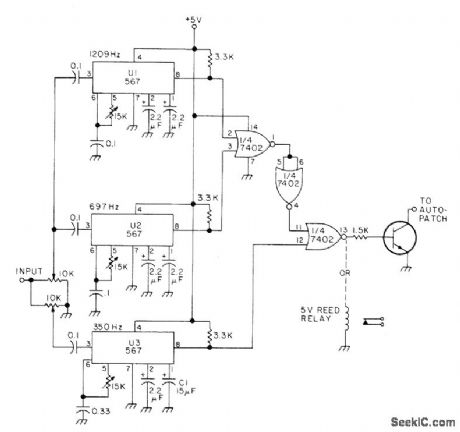
Prevents unauthorized direct long-distance dialing through repeater autopatch from areas where 1 must be dialed ahead of desired out-of-town phone number. Based on simultaneous detection of 350-Hz component of dial tone and 1209- and 697-Hz tones assigned to 1 in Touch-Tone system. Circuit requires only three 567 tone decoders, 7402 quad gate, and either transistor or relay for controlling autopatch. Article covers installation and operation.-W. J. Hosking, Long Distance Call Eliminator, 73 Magazine, April 1976, p 44-45. (View)
View full Circuit Diagram | Comments | Reading(618)
PULSE_SHAPER_FOR_FREQUENCY_MULTIPLIER
Published:2009/7/15 2:36:00 Author:Jessie

Combines clipping with cathode peaking to increase rise time to 1 microsec for 150.v pulses that drive blocking oscillator.-W. O. Brooks, Stepping up Frequency with Counter Circuits, Electronics, 32:29, p 60-62. (View)
View full Circuit Diagram | Comments | Reading(679)
PLL_SINGLE_TONE_DECODER
Published:2009/7/14 6:49:00 Author:May


Can be used for Touch-Tone decoding as well as for telephone-line and wireless control applications using single audio frequency. Operating center frequency depends on H1 and C1. R1 should be between 2K and 20K. C1 in microfarads is computed from f = 1/R1C1, where R is in megohms and f is in hertz. C2 is low-pass filter in range of 1-22μF; the larger its value, the narrower its bandwidth. C3 is not critical and can be about twice C2.-C. D. Rakes, Integrated Circuit Projects, Howard W. Sams, Indianapolis, IN, 1975, p 68-73. (View)
View full Circuit Diagram | Comments | Reading(775)
HIGH_VOLTAGE_PULSE_DELAY
Published:2009/7/15 2:36:00 Author:Jessie

Diode input network isolates base of Q1 from input when input pulse voltages exceed maximum rated emitter-to-base reverse voltage of input inverting digital pulse delay circuit.-R. A. Karlin, One-Transistor Multi Delays Digital Pulses, Electronics, 38:17, p 85-86. (View)
View full Circuit Diagram | Comments | Reading(976)
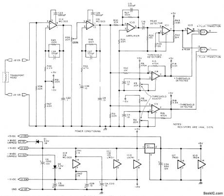
DIGITAL_CASSETTE_READ_AMPLIFIER
Published:2009/7/14 6:46:00 Author:May
Signal from magnetic head of digital tape cassette is amplified by two-stage MC1303 amplifier providing analog output of about 4 V P-P to μA741 opamp IC10 of LM311 peak detector 1C11. Signal also goes to LM311 positive and negative threshold detectors is low; above reference, output is high. Negative threshold detector operates similarly for negative pulses. Time jitter in outputs is eliminated by detecting peak of analog read signal, then combining result with threshold in. formation in peak detector. Circuit is used ; Phi-Deck cassette system made by Economy Company, Oklahoma City.-I, Rampil and J. Breimeir, The Digital Cassette Subsystem: Dig-ital Recording Background and Head Interface Electronics, BYTE, Feb. 1977, p 24-31. (View)
View full Circuit Diagram | Comments | Reading(1552)
INTERFACE_FOR_AUDIO_CASSETTES
Published:2009/7/14 6:42:00 Author:May

Permits use of ordinary home cassette recorder to provide high-speed loading of assembler and source program into microprocessor. Data is recorded by using variation of phase encoding, which provides self-clocking and is independent of tape speed variation. Effective I/O rate is about 500 b/s or 5 times that of low-speed paper-tape punch or reader. Article covers phase-encoding procedure, gives flowchart, and shows waveforms of pulses at five points in circuit. Parity bits provide error correction and detection, using Hamming code.-S. Kim, An Inexpensive Audio Cassette Recorder Interface for, μP's, EDN Magazine, March 5, 1976, p 83-86. (View)
View full Circuit Diagram | Comments | Reading(569)
KEY_PULSER
Published:2009/7/14 6:16:00 Author:May

American Microsystems S2560A CMOS IC pulser converts pushbutton inputs to series of pulses suitable for telephone dialing, as replacement for mechanical telephone dial. Circuit shows typical connection to dial telephone set using 500-type encapsulated circuit. Dialing rate can be varied by changing dial rate oscillator frequency. IC includes 20-digit memory that makes last dialed number available for redialing until new number is entered, Entered digits are stored sequentially in internal memory, with dial pulsing starting as soon as first digit is entered. Arrangement permits entering digits much faster than output rate. Last number is redialed by going off hook and pressing # key.- Key Pulser, American Microsystems, Santa Clara, CA, 1977, S2560A/S2560B, p 8. (View)
View full Circuit Diagram | Comments | Reading(1432)
| Pages:617/2234 At 20601602603604605606607608609610611612613614615616617618619620Under 20 |
Circuit Categories
power supply circuit
Amplifier Circuit
Basic Circuit
LED and Light Circuit
Sensor Circuit
Signal Processing
Electrical Equipment Circuit
Control Circuit
Remote Control Circuit
A/D-D/A Converter Circuit
Audio Circuit
Measuring and Test Circuit
Communication Circuit
Computer-Related Circuit
555 Circuit
Automotive Circuit
Repairing Circuit