
Circuit Diagram
Index 604
HIGH_INPUT_IMPEDANCE
Published:2009/7/14 20:52:00 Author:May

Gives current gain of 1,000, voltage gain of 40, input impedance of0.4 meg, and good short-term temperature stability. Output stage is battery-coupled.-D. Schuster, D-C Transistor Amplifier for High-Impedance Input, Electronics, 31:9, p 64-66. (View)
View full Circuit Diagram | Comments | Reading(0)
SIMPLE_TRIANGLE_WAVEFORM_GENERATOR
Published:2009/7/14 23:30:00 Author:Jessie

This triangle-waveform generator was designed to give good results with as few parts as possible. (View)
View full Circuit Diagram | Comments | Reading(1618)
EQUIPMENT_INTERFACE_PROTECTION
Published:2009/7/14 23:29:00 Author:Jessie

When circuit shown is used to transfer signal from one piece of equipment to another, desired signal passes with very little degradation. Component values can be chosen to make thyristor SCP1 latch at any desired voltage between A and B that is greater than 0V, blowing fuse F1 and giving desired protective isolation. On other side of circuit, SCR2 will latch and blow F2 when voltage exceeds limiting value set by diode D2 and zener D4. Zeners are 10-V CV7144, diodes are CV9637 small-signal silicon, resistors are 10K, capacitors are 0.047 μF, and thyristors are 2N4147.-S. G. Pinto and A. P. Bell, Thyristor Protection Circuit, Wireless World, Oct. 1975, p 473. (View)
View full Circuit Diagram | Comments | Reading(677)
CURRENT_MODE_LOGIC_FOR_500_MC_GATED_FLIP_FIOP
Published:2009/7/14 20:51:00 Author:May

Uses 2N2475 Transistors and 1N3859 tunnel diodes in current mode logic circuit having four inputs that can be energized to provide variety of desired logic functions. Supply of 0.8 v is obtained by passing current through two forward silicon diodes. Narrow 1-nsec clock pulse is generated by snap diode as close as possible to tunnel diode.-R. Glasgal , 500 MHz Transistor-TD Gated Flip Flop, EEE, 14:1, p 98-101. (View)
View full Circuit Diagram | Comments | Reading(763)
ATTACK_DECAY_RAMP_GENERATOR
Published:2009/7/14 23:29:00 Author:Jessie

In the circuit diagram shown, a digital-to-analog converter (DAC) IC is used to create an envelope waveform, the attack and decay of which are controllable. Typical applications can include audio and music synthesizer circuitry. Its operation is as follows. IC1a and IC1b form two variable-frequency oscillators, whose outputs are fed to IC2. This is configured as a demultiplexer, addressed by a signal appearing on pin 11. The signal from IC1a or IC1b appears at the output, pin 3. Initially pin 11 of IC2 will be high, so IC1a will be selected and fed through resistor R1 to IC4, a bi-nary counter, which is cascaded to 106. In total, this results in an 8-bit binary count (0 to 255) appearing at the counters' outputs. The speed of the count is adjustable with VR1. The counter output is fed directly to IC3, a ZN429E digital-to-analog converter. The ramp voltage appears at pin 4 of IC3, and will always be between 0 and 4 V. When the counter reaches its terminal count of 255, pin 7 of IC6 (CARRY OUT) will go low. This signal is inverted by IC1c and used as a clock pulse to IC5, a 4013 D-type flip-flop. The output at pin 1 of IC5 now goes low, so that a logic 0 is placed on pin 11 of IC2 and on pin 10 (UP/DOWN) of both counter ICs. Oscillator IC1b is now fed through the dernultiplexer to the counters, which now count down from 255. The output voltage from IC3 will now fall at a rate determined by the setting of VR2. As the count passes zero and rolls back to 255, a pulse again appears at pin 7 of IC6, and the cycle continues. At any time, switch S1 (debounced by CB and R3) can be momentarily activated. This causes a high output at pin 13 of IC5, which drives transistor TR1, shunting the clock signal to the counters. This will freeze the count at that point. A second operation of S1 restarts the count from where it left off. A buffer/amplifier formed by IC8a (one half of an LM358N) allows the output voltage of the DAC (IC3) to be increased or the dc level shifted. (View)
View full Circuit Diagram | Comments | Reading(1762)
FAIL_SAFE_TTL_INTERFACE
Published:2009/7/14 20:51:00 Author:May

Diode and FET protect SN74121 high-speed level detector from excessive opamp output voltage. If input of opamp goes too far negative, positive-going output will cause breakdown of TTL input. Protective interface makes circuit fail-safe without loss of operating speed. D, should be highspeed germanium diode with breakdown volt-age above highest positive output of amplifier (usually about 15 V).-K. I. Wolfe, A Safer Analog-to-Digital Interface, EDN Magazine, March 5, 1974, p 74. (View)
View full Circuit Diagram | Comments | Reading(638)
INTERMEDIATE_FREQUENCY_TRANSMITTER
Published:2009/7/14 20:50:00 Author:May
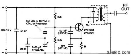
The oscillator transmitter circuit is a variation of the Colpitts configuration. This particular circuit exhibits excellent frequency stability, good isolation between the frequency reference and the output, and isolated low output impedance. If you have the correct crystal on hand, that's fine. If not, a ceramic resonator will also work with the components shown. The tuned circuit T1 is an IF can, salvaged from an old AM and FM receiver; be sure that it has a primary tap. The primary of the 455-KHz, IF can will measure 3 to 5Ω, and the 10.7-MHz IF can will measure less than 1Ω; these measurements will help you to identify the correct inductor. The components in parentheses should be used for the 455-kHz transmitter. (View)
View full Circuit Diagram | Comments | Reading(2470)
NOR_FUNCTION_RESET
Published:2009/7/14 20:49:00 Author:May

Modified flip-flop is set or reset when all input signals are low, corresponding to nor-function of input signals rather than the usual or function,-L. Mercurio, Flip-flop Operated by Input Signal NOR, EEE, 3:12,p 65. (View)
View full Circuit Diagram | Comments | Reading(647)
STARTER_FOR_FLIP_FLOP
Published:2009/7/14 20:49:00 Author:May

Free-running flip-flop (thin lines) has several desired features but will not start oscillation by itself. Output impedance is less than 1,800 ohms, period is 1 millisec, and circuit is quite stable once in operation. Heavy lines show additions re quired for starting flip-flop when it is stalled.C3 (150 mfd) is in circuit for time period in which power supply voltage increases from 0 to 9 v after switch is dosed. Relay pulls in at 9 v, to remove C3 from circuit after it has served its starting function.-Starter Circuit for Flip-Flop, Electronic Circuit Design Handbook, Mactier Pub. Corp., N.Y., 1965, p 229. (View)
View full Circuit Diagram | Comments | Reading(593)
TONE_ENCODER
Published:2009/7/14 20:48:00 Author:May

Motorola MC14410 CMOS IC is basis of accurate low-power Touch-Tone encoder system providing full 2-of-8 encoding from basic 1-MHz crystal oscillator. Can be used with 2-of-7 or 2-of-8 keypad switch matrix such as Chromerics ER-21623 or ER-21611. Q1-Q2 form tone-amplifiet/emitter-follower line driver. U2 is push-to-talk mono 1-s timer. Supply can be any voltage from 5to 12V if zener is used to supply 5 V to ICs. Article covers circuit operation in detail and gives tone-encoder frequency table.-J. DeLaune, Digital Touch-Tone Encoder for VHF FM, Ham Radio, April 1975, p 28-31.
(View)
View full Circuit Diagram | Comments | Reading(0)
AUDIO_PROCESSOR_FOR_RTTY_RECEIVER
Published:2009/7/14 23:29:00 Author:Jessie

Audio tones of 2125 and 2975 Hz, as received and detected by FM receiver, are limited and fed to two active bandpass filters, each set to one of tone frequencies. Outputs are amplitude-detected and compared, to give output of 1 for 2125 Hz and output of 0 for 2975 Hz. Output is suitable for UART providing serial-to-parallel conversion,-D. Lancaster, TV Typewriter Cookbook, Howard W. Sams, Indianapolis, IN, 1976, p 174-175. (View)
View full Circuit Diagram | Comments | Reading(715)
MONOSTABLE_DELAY
Published:2009/7/14 23:28:00 Author:Jessie

Designed to perform delay function in digital logic circuits for computer, control, and communication equipment. Choice of feedback capacitor C1 gives delay range from 2microsec to 100 millisec.R3 may be made variable for further adjustment of time delay.-NBS, Handbook Preferred Circuits Navy Aeronautical Electronic Equipment, Vol. II, Semiconductor Device Circuits, PSC 10 (originally PC 213), p 10-2. (View)
View full Circuit Diagram | Comments | Reading(788)
BIPOLAR_OUTPUT
Published:2009/7/14 20:48:00 Author:May

Output is dean square wave whose symmetry with respect to ground can be balanced by potentiometer R18. When input is fed by pulse generator, output can be used to test frequency re sponse of transistor circuits.-F. C. Ruegg, Multivibrator Provides Bidirectional Output Pulses, Electronics, 38:17, p 87. (View)
View full Circuit Diagram | Comments | Reading(0)
GROUND_FAULT_INTERRUPTER
Published:2009/7/14 23:27:00 Author:Jessie

Compares current in ungrounded side of power line with current in neutral conductor. If currents are not equal, ground fault exists because portion of line current is taking an unintended return path through leaky electric appliance or human body. Voltage induced in toroid by unbalanced current is amplified for energizing relay K1 to break circuit. Toroid uses Amidon T-184-41 core, with 600 turns No. 30 for secondary, and 12 turns No. 16 solid twisted-pair for primary. Circuit operates on fault current of 4mA, well below danger limit for children.-W. J, Prudhomme, The Unzapper, 73 Magazine, Nov./ Dec. 1975, p 151-156.
(View)
View full Circuit Diagram | Comments | Reading(1166)
PREFERRED_FAST_RECOVERY_PHANTASTRON_DELAY
Published:2009/7/14 23:26:00 Author:Jessie


Generates rectangular waveform whose duration is almost directly proportional to control signal. Used to produce movable markers on radar display and to time-modulate pulse in accordance with variable quantities such as antenna position. Maximum recovery time is 40microsec. Control signal is 20 to 240V .input 1 is -15V,and input 2 is -10V.-NBS. Handbook Preferred Circuits Navy Aeronautical Electronic Equipment. Vol.1,Electron Tube Circuits,1963,PC 57,p57-2. (View)
View full Circuit Diagram | Comments | Reading(606)
STRAIN_GAGE_OSCILLATOR
Published:2009/7/14 23:26:00 Author:Jessie


Produces f-m signal output that is directly proportional to applied force, such as stress or pressure resistive-type gage. Operating and band, edge frequencies of oscillator are determined by values of R, L, and C.-W. H. Foster, Strain Gage Oscillator for Flight Testing, Electronics, 31:5, p 40-42. (View)
View full Circuit Diagram | Comments | Reading(727)
QUADRATURE_OSCILLATOR_USES_MULTI
Published:2009/7/14 20:48:00 Author:May

PLIERS-4214 differential multipliers eliminate need for opamps in quadrature oscillator in which frequency is controlled by external DC voltage. R3, R4, R5, and D1 form diode limiter, while R1,R2,and C1,provide positive feedback to sustain oscillation,R1 should be about equal to R, R2about 20R, and C1 about 10C. R2 can be readjusted for best compromise between distortion and speed of amplitude buildup.-Y. J. Wong, Design a Low Cost, Low-Distortion, Precision Sine-Wave Oscillator, EDN Magazine, Sept. 20, 1978, p 107-113. (View)
View full Circuit Diagram | Comments | Reading(962)
160_MC_15_W_POWER_AMPLIFIER
Published:2009/7/14 23:25:00 Author:Jessie
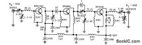
Performance of each of three stages is optimized by using input-output admittance data in network design, to give 30.5 db power gain front class-C operation. Circuit can be expanded to give complete f-m or c-w transmitter by adding appropriate oscillator-buffer-multiplier stages.-R. Hejhall, A 160 MHz 15.Watt Solid-State Power Amplifier, Motorola Application Note AN-214, Nov.1965. (View)
View full Circuit Diagram | Comments | Reading(1988)
400_MC_VARICAP_OSCILLATOR
Published:2009/7/14 23:24:00 Author:Jessie

Wideband frequency modulation of 400-Mc distributed-parameter Colpitts oscillator is obtained with symmetrical transistor in modulator. Q1 is equivalent to two reverse, biased diodes in series for r-f and in parallel with respect to modulating signals and d-c bias.-C. Arsem, Wideband r-m with Capacitance Diodes, Electronics, 32:49, p 112-113. (View)
View full Circuit Diagram | Comments | Reading(818)
FSK_GENERATOR_1
Published:2009/7/14 23:23:00 Author:Jessie

Digital programming capability of Exar XR-215 PLL IC is used to provide shifting of VCO frequency between mark and space frequencies by applying logic pulse to pin 10. Circuit gives 2.5 V P-P output at pin 15 and 1O V P-P output at pin 8, Each output is symmetrical square wave with second harmonic content less than 0.3%. - Phase-Locked Loop Data Book. Exar Integrated Systems, Sunnyvale, CA, 1978, p 21-28. (View)
View full Circuit Diagram | Comments | Reading(799)
| Pages:604/2234 At 20601602603604605606607608609610611612613614615616617618619620Under 20 |
Circuit Categories
power supply circuit
Amplifier Circuit
Basic Circuit
LED and Light Circuit
Sensor Circuit
Signal Processing
Electrical Equipment Circuit
Control Circuit
Remote Control Circuit
A/D-D/A Converter Circuit
Audio Circuit
Measuring and Test Circuit
Communication Circuit
Computer-Related Circuit
555 Circuit
Automotive Circuit
Repairing Circuit