
Circuit Diagram
Index 602
SCR_UJI_TIME_DELAY
Published:2009/7/14 23:50:00 Author:Jessie

Timing interval is initiated by applying power, and is determined by RT-CT. At end of interval, unijunction transistor triggers silicon controlled rectifier, to apply essentially full supply voltage to load. Delay range is from 0.4millisec to 1 minute.- Transistor Manual, Seventh Edition, General Electric Co.1964, p 321. (View)
View full Circuit Diagram | Comments | Reading(734)
WIRELESS_CAMCORDER_MICROPHONE
Published:2009/7/14 21:06:00 Author:May

A 741 op amp acts as an audio amplifier and frequency-modulates VHF oscillator Q1 via varactor D2. L1 is 2.5 turns of #18 wire on a 5/16,-inch-diameter form. The turn spacing can be varied to adjust the transmitter frequency. ' (View)
View full Circuit Diagram | Comments | Reading(1701)
DELAY_MULTIPLIER
Published:2009/7/14 23:48:00 Author:Jessie

Addition of silicon unijunction transistor Q3 to conventional mono stable mvbr expands time delay two orders of magnitude.-M. P. Humblet, Unijunction Transistor Multiplies Monostable 's Pulsewidth, Electronics, 35:26, p 74-75. (View)
View full Circuit Diagram | Comments | Reading(655)
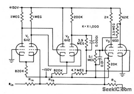
15_W_TRANSFORMERLESS_AMPLIFIER
Published:2009/7/14 23:47:00 Author:Jessie

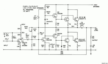
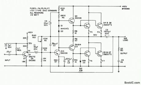
Uses additional input stage to increase input impedance from 3K to over 200K.Power frequency response is flat within 0.5 db from 20 cps to 20 kc. Output impedance is less than 0.3 ohms, for good speaker damping,and harmonic distortion at full power is less than 0.25%.- Transisfor Manual, Seventh Edition, General Electric Co., 1964, p 269. (View)
View full Circuit Diagram | Comments | Reading(890)
HARMONIC_GENERATOR
Published:2009/7/14 23:47:00 Author:Jessie

This simple circuit acts as a frequency multiplier, which converts any sloped input waveform into a distorted output waveform, whose frequency spectrum is marked by a rich harmonics content.The input frequency does not disappear from the spectrum, however. When a pure sine-wave input signal is applied, the circuit generates odd harmonics only. The push-pull outputs of comparators IC1b and IC1a then supply differential signals to adder IC2, which cancels out even-numbered harmonics. For different mark/space ratios of the output signals, as set with P1 and P2, the harmonic spectrum changes. A duty factor of 0.25, for instance, will cause the circuit to supply the second, sixth, and tenth harmonics, but not the fourth one. The spectrum function is then written as sin x/x.The reference levels for the input comparators determine the output waveform. The desired degree of distortion of the input waveform is, therefore, adjusted with the two presets. R2 and R3 should be matched to within 1 percent. (View)
View full Circuit Diagram | Comments | Reading(3377)
BYPASSING_SOLENOID_TRANSIENTS
Published:2009/7/14 23:46:00 Author:Jessie

Feedback from collector to base of power transistor through C1 and R2 protects device from destructive transients generated when inductive load such as solenoid is turned off. Alternative use of diode CR2 or CR1-R1 across coil would limit voltage transient but would increase solenoid release time.-D. Thomas, Feedback Protects High-Speed Solenoid Driver, EDN Magazine, Jan. 1, 1971, p 40.
(View)
View full Circuit Diagram | Comments | Reading(875)
POWER_SUMMING_D_C_AMPLIFIER
Published:2009/7/14 21:05:00 Author:May
Open loop gain is 2,000 and maximum voltage swing is 10V into 2,000-ohm load. Maximum dosed-loop gain should be 50 for good stability. Used for straight resistance summing of several input signals.-L. S. Klivans, D.C Amplifiers for Control Systems, Electronics, 31:47, p 96-100. (View)
View full Circuit Diagram | Comments | Reading(676)
250_KC_FLIP_FLOP
Published:2009/7/14 21:05:00 Author:May

Basic design procedure is given. Circuit shown operates over temperature range of -55 to +55℃ with input frequency of 250 kc.-Texas Instruments Inc., Transistor Circuit Design, McGraw-Hill, N.Y., 1963, p 377. (View)
View full Circuit Diagram | Comments | Reading(735)
MULTCHIP_COMPLEMENTARY_FLIP_FLOP
Published:2009/7/14 21:04:00 Author:May


Circuit for microelectronic application allows use of most suitable substrate for each component.-J. Eimbinder, Multichip Circuits Get Off The Ground, Electronics, 37:25, p105-107. (View)
View full Circuit Diagram | Comments | Reading(616)
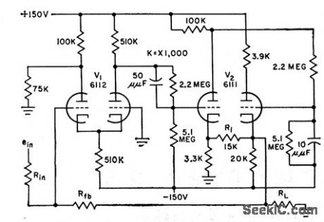
OPERATIONAL_D_C_AMPLIFIER
Published:2009/7/14 21:04:00 Author:May
Ideal for control systems and analog computers because of broad passband and large control-system response characteristic. Open-loop gain above 15,000. Output swings 100V into 20,000-ohm load. Can be used from d-c to 20kc at unity dosed-loop gain.-L. S. Klivans, D-C Amplifiers for Control Systems, Electronics, 31:47, p 96-100. (View)
View full Circuit Diagram | Comments | Reading(719)
NONSATURATED_FLIP_FLOP
Published:2009/7/14 21:00:00 Author:May

Design procedure is given in 52 steps for manufacturability and long-term reliability, making full allowance for component tolerances, voltage fluctuation, and collector output loading.- Transistor Manual, Seventh Edition, General Electric Co., 1964, p 189. (View)
View full Circuit Diagram | Comments | Reading(643)
FAN_OUT_TO_60
Published:2009/7/14 20:59:00 Author:May

Fan-out of conventional flip-flop is quadrupled by driving bases of amplifiers Q1 and Q2 directly from emitters of Q3 and Q4.-D. J. Grover, Modified Flip-flop Quadruples Fan-Out, Electronics, 38:26, p 67-68. (View)
View full Circuit Diagram | Comments | Reading(576)
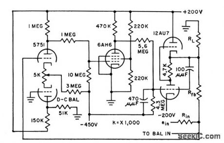
4OO_CPS_SUMMING_AND_POWER_AMPLIFIER
Published:2009/7/14 20:58:00 Author:May
Used in either 60 or 400-cps control systems in which several signals must be summed and amplified in precise manner. Also used for broadband equalization when load impedance is below 25,000 ohms and phase lag must be minimum. Phase shift is less than 5° from d-c to 400 cps. Open-loop gain is above 5,000.-L. S. Klivans, D-C Amplifiers for Control Systems, Electronics, 31:47, p 96-100. (View)
View full Circuit Diagram | Comments | Reading(675)
CURRENT_SENSOR
Published:2009/7/14 23:45:00 Author:Jessie
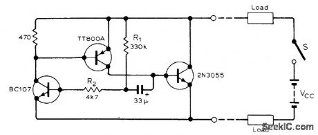
Load current is sensed across base-emitter junction of output transistor. R1 controls OFF time and R2 controls ON time. Capacitor should be electrolytic rated above 16V.-M, Faulkner, Two Terminal Circuit Breaker, Wireless World, March 1977, p 41. (View)
View full Circuit Diagram | Comments | Reading(1264)
AM_TONE_TRANSMITTER
Published:2009/7/14 20:58:00 Author:May
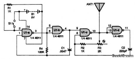
Power for the circuit is supplied by B1, a 9-V battery. Two sections of a 4011 NAND gate, U1-c and U1-d, are used as part of a radio-frequency (RE) oscillator (carrier). The other two sections, U1-a and U1-b, are used in an audio-frequency (AP) oscillator (modulator). Switch S1 enables and disables the modulation to allow the transfer of an intelligent message with the transmitter. When you press S1, the AP oscillator composed of U1-a, U1-b, R4, and C1 starts generating an audio signal.That signal gates the RE oscillator composed of U1-c, U1-d, R2, R3, and C2 on and off. When on, the RE oscillator runs at 1 MHz. The resulting output is sent out ANT1 as an AM signal. (View)
View full Circuit Diagram | Comments | Reading(2438)
LOOSE_GROUND_FLASHER
Published:2009/7/14 23:43:00 Author:Jessie

Uses ordinary neon lamp in series with silicon diode, with lamp normally dark. Gives warning by flashing if ground wire is accidentally or purposely disconnected from chassis of oscilloscope or other test instrument,-R. H. Troughton, Earth Warning Indicator, Wireless World, April 1977, p 62.
(View)
View full Circuit Diagram | Comments | Reading(861)
UART_INTERFACE
Published:2009/7/14 23:43:00 Author:Jessie

Permits use of universal asynchronous receiver-transmitter with model 33 Teletype so keyboard can send and printer can receive at same time. Transmitter interface provides 20-mA current for mark or 1 and open circuit for space or 0. Receiver senses closed contact for mark or 1 and open contact for space or 0. Extra inverters are added to make codes correspond so 1 from UART is read as 1 by Teletype. Designed for 110-baud rate.-D. Lancaster, TV Typewriter Cookbook, Howard W. Sams, Indianapolis, IN, 1976, p 162-164. (View)
View full Circuit Diagram | Comments | Reading(0)
UNDERVOLTAGE_ALARM
Published:2009/7/14 20:56:00 Author:May

3905 timer output goes high when power supply drops below predetermined voltage level. Timer is connected as inverting comparator that compares fraction of supply voltage (as set by R1) with fixed voltage-comparison threshold of 2 V for timer. Output can be used to drive suitable alarm indicator.-W. G. Jung, IC Timer Cookbook, Howard W. Sams, Indianapolis, IN, 1977, p 230-231. (View)
View full Circuit Diagram | Comments | Reading(1111)
PROGRAMMABLE_PULSE_GENERATOR
Published:2009/7/14 23:43:00 Author:Jessie

This circuit provides a programmable flat-pulse generator with TTL input and up to 24 V p-p output with a 2500-V-μs slew rate. Clamp amplifiers are useful as protective buffers for A/D inputs, as programmable flat-pulse-forming amplifiers, and as amplitude modulators. Because VH and VL clip in the in-put stage and have input bandwidths comparable to the signal inputs, they can also be used in simple circuitry to generate the positive or negative absolute value of input signals (i.e., full-wave rectify them). (View)
View full Circuit Diagram | Comments | Reading(1527)
FAIL_SAFE_INTERLOCK
Published:2009/7/14 23:43:00 Author:Jessie


Developed for protecting people and equipment at 40-kW RF accelerator station. All interlock switches (air flow, water flow, water pressure, temperature, etc) are normally closed, grounding one side of each relay coil. All relays are normally pulled in, to provide complete interlock chain. Failure of any component, including power supply, breaks chain and places system in safe mode.-T. W. Hardek, Interlock Protection Circuit Is Simple and Fail-Safe, EDN Magazine, May 20, 1975, p 74. (View)
View full Circuit Diagram | Comments | Reading(1284)
| Pages:602/2234 At 20601602603604605606607608609610611612613614615616617618619620Under 20 |
Circuit Categories
power supply circuit
Amplifier Circuit
Basic Circuit
LED and Light Circuit
Sensor Circuit
Signal Processing
Electrical Equipment Circuit
Control Circuit
Remote Control Circuit
A/D-D/A Converter Circuit
Audio Circuit
Measuring and Test Circuit
Communication Circuit
Computer-Related Circuit
555 Circuit
Automotive Circuit
Repairing Circuit