
Circuit Diagram
Index 600
CMOS_ULTRASONIC_GENERATOR
Published:2009/7/14 21:18:00 Author:May
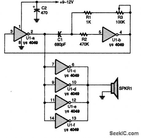
This ultrasonic generator uses a single CD4049IC. The frequency range is about 15 to 50 kHz. (View)
View full Circuit Diagram | Comments | Reading(2316)
SOLENOID_PUMP_PULSER
Published:2009/7/14 21:17:00 Author:May

Scr flip-flop feeds 5-amp pulses altenately to two solenoid pump coils at rates varying from 1.5 to 25 cps.-U. L. Upson, Solid-State Pulser Drives Chemical Pump, Electronics, 33:49, p 74-76. (View)
View full Circuit Diagram | Comments | Reading(625)
SELF_INDICATING_FLIP_FLOP
Published:2009/7/14 21:17:00 Author:May

Uses Amperex 6679 triode having fluorescent anode, to eliminate need for neons as indicators. Incorporates collector protection and stabilization against beta variation of transistor.-H. Rodriques deMiranda and I. Rudich, Indicator Triode for Direct Data Readout, Electronics, 33:6, p 52-54. (View)
View full Circuit Diagram | Comments | Reading(604)
CRT_TUNING_INDI_CATOR
Published:2009/7/15 2:08:00 Author:Jessie

Crossed -ellipse display on CRT aids in tuning receiver to RTTY signal. Display shows at a glance if station is narrow or wide, or if other station is transmitting upside-down signals (mark and space frequencies reversed). Tuned for maximum amplitude of major axis of each ellipse; if transmitting station is wide or narrow, tune for equal amplitudes even though they are not maximized. Try different values of RV until T.P.1 voltage is 65 V, to center signal so it can swing equal amounts on either side Adjust RH similarly-R.R. Parry, RTTY CRT Tuning Indicator, 73 Magazine, Sept 1977, p 118-120. (View)
View full Circuit Diagram | Comments | Reading(1243)
SLOW_MAKE_RELAY
Published:2009/7/14 23:37:00 Author:Jessie

Circuit energizes relay with delay controlled by R2-C1 after driving pulse is applied. Relay de-energizes the instant driving pulse is removed.-P. Haas, Timing Circuits Control Relays, Electronics, 38:6,p85. (View)
View full Circuit Diagram | Comments | Reading(751)
A_F_OUTPUT_TRANSISTOR_PROTECTION
Published:2009/7/14 22:48:00 Author:Jessie

When output of 3-w audio amplifier is short-circuit,protection circuit reduces overall gain by 20 db.-E. Segatis, Circuit Protects Amplifier Against Short Circuit,Electronics,37:23,p 61-62. (View)
View full Circuit Diagram | Comments | Reading(708)
AC_LINE_ZERO_CROSSING_DETECTOR
Published:2009/7/14 22:48:00 Author:Jessie

Positive-going half-cycles forward-bias D1, allowing capacitor to charge through D3 to 14V. Negative half-cycles forward-bias D2 allowing capacitor to charge through D3 to 14 V. Negative half-cycles forward-bias D2 to turn on Tr1 and discharge capacitor. Output is about 1 V less on negative half-cycles. Transistor and diode types are not critical, except that D1 must withstand full reverse voltage of AC line.-R. J. Torrens, Zero Crossing Detector, Wireless World, Jan.1977, p 78.
(View)
View full Circuit Diagram | Comments | Reading(945)
8_W_SILICON_TRANSISTOR_POWER_AMPLIFIER
Published:2009/7/14 22:48:00 Author:Jessie
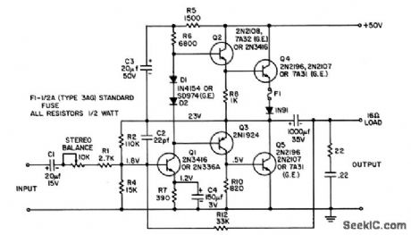
Output impedance is 0.5 ohm, for good speaker damping,Response is down only 3 db at 86 kc.Power response is flat Within 0.33 db from 30 cps to 15 kc at 6 w output.- Transistor Manucal, Seventh Edition, General Electric Co., 1964, p 263. (View)
View full Circuit Diagram | Comments | Reading(1121)
WIDE_BANDWIDTH_VOLTAGE_TO_FREQUENCY_CONVERTER
Published:2009/7/14 22:47:00 Author:Jessie

Shown is the design for a low-cost, wide-bandwidth voltage-to-frequency converter (VFC). The core element of the prototype VFC is a Maxim MAX942 high-speed comparator. When operating, R1, R2, and R3 provide hysteresis with trip points from one-third to two-thirds of the supply voltage.This permits wide adjustability in the width of the output pulse. Q1C and Q1B form a current mirror that linearizes the charge potential across C2. As the voltage at pin 2 of U1 crosses the lower trip point, the comparator output turns on. The current mirror sink node is raised above the program voltage, which turns it off. D1 turns on, removing the charge on C2 through R4. When the voltage at U1 pin 2 crosses the upper trip point, the circuit resets. Upon observation, the prototype circuit linearity was approximately 2 percent over the tested range. Also, up to 6-MHz operation was possible using the MAX942 by carefully selecting C2 and the hysteresis resistors. Discrete transistors can be used instead of the Motorola MPQ2N2222 monolithic quad package. This can cause some instability at low frequencies. The transistors should be located in close thermal proximity. On the high side, a good, matched transistor pair can be used. Analog Devices' MAT-01 is a good choice. (View)
View full Circuit Diagram | Comments | Reading(2339)
GATE_TURNOFF_SCR_FLIP_FLOP
Published:2009/7/14 21:16:00 Author:May

Capacitor-commutated flip-flop transfers current front one load to other each time positive trigger pulse is applied to common input line, at rates up to 10 kc.-D. It. Grafham, Now the Gate Turnoff Switch Speeds Up D-C Switching, Electronics, 37:12, p 64-71. (View)
View full Circuit Diagram | Comments | Reading(986)
ULTRASONIC_MOTION_DETECTOR
Published:2009/7/14 21:16:00 Author:May
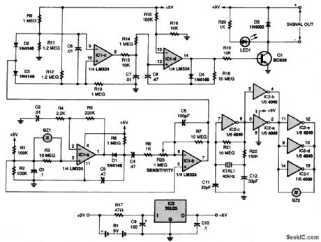
The receiver section of the circuit is made up of four ac-coupled stages, each built around one of four sections of an LM324 op amp, IC1. At the input to the third stage-a differential amplifier built around IC1-c-are two diodes, D2 and D3. They detect both positive and negative pulses. When there is no movement, the voltage at pin 7 of IC1-b is half the supply voltage and neither D2 or D3 can conduct. The voltage at pin 8 of IC1-c is then low. If the signal rises above +0.7 V, D3 conducts, causing the output on pin 8 to go high. If the signal falls below -0.7 V, D2 conducts, which also causes the output to go high. The fourth stage, built around IC1-d, is set up as a monostable flip-flop. That stage converts any signal that gets through the filter into a pulse substantial enough to turn on transistor Q1. When Q1 conducts, LED1 turns on and an output signal is provided to drive a separate relay or any other device connected to the circuit (View)
View full Circuit Diagram | Comments | Reading(0)
FLIP_FLOP_DRIVES_GALLIUM_ARSENIDE_LAMP
Published:2009/7/14 21:16:00 Author:May

Pulses from mvbr (not shown) trigger flip-flop that feeds 1-amp current pulses to GaAs lamp through emitter-follower and power transistor. Used in high-speed punched tape, reader.-R. F. Broom and C. Hilsum, Diode Lamp Makes Tape Readers Easter, Electronics,36:20,p 44-45. (View)
View full Circuit Diagram | Comments | Reading(839)
TOUCH_TONE_IC
Published:2009/7/14 21:14:00 Author:May

MOSTEK MK5085/6 IC and keyboard together form inexpensive Touch-Tone generator producing tones within 0.75% of required values. Uses 3.579545-MHz TV color-burst crystal. Pin 15 is grounded to provide dual tones only .Pin 10 provides output when keyboard entry has been made ,for keying push-to-talk (PTT) Loudspeaker can be eliminated if output if fed directly into microphone input of transmitter. Choice of IC depends on type of keyboard used.-T. Ahrens, Integrated-Circuit Tone Generator, Ham Radio, Feb. 1977, p70. (View)
View full Circuit Diagram | Comments | Reading(2808)
TOUCH_SWITCH_II
Published:2009/7/14 19:57:00 Author:May

IC1, a 555 timer, is connected in a one-shot multivibrator circuit that is triggered by touching the touch terminal. The timed ON period is about 4 seconds with the component values given. To increase the ON time, increase the value of R3 or C2; to decrease the ON time, reduce the value of R3 or C2. The 9-V output at IC1 pin 3 can be used to drive an optocoupler, a power transistor, a hexFET transistor, CMOS circuitry, and more. (View)
View full Circuit Diagram | Comments | Reading(0)
LASER_CURRENT_MODULATION
Published:2009/7/14 11:50:00 Author:May

Depending on laser characteristics, only a small percentage of modulation (around 10 percent) is possible with this scheme. (View)
View full Circuit Diagram | Comments | Reading(672)
WEATHER_VANE
Published:2009/7/15 0:22:00 Author:Jessie

IC1-a and IC1-b form an astable oscillator in which IC1-a produces a positive pulse width that is proportional to the resistance of the segmented potentiometer, R1. The negative pulse width, deter-mined by IC1-b, is fixed. The third section, IC1-c, is triggered by the falling edge of IC1-b. Its pulse width is set by potentiometer R7 so that it is exactly equal to the width of the IC1-a's pulse when the vane is at zero resistance. Potentiometer R8 and IC1-d make up the frequency reference. An astable oscillator (formed out of IC1-d and its surrounding components) provides a clock signal to IC2, a 555 timer IC. The RESET pulse from IC1-c starts to count at zero, and the LATCH pulse from IC1-a freezes the instantaneous reading in the timer. So, U2 counts the time between the falling edge of IC1-a and the falling edge of IC1-c, which is determined by the position of the vane. The timer can feed its digital output to the three-digit display circuit of your choosing (such as an MC4511 display driver). To adjust the circuit, rotate RI (the transducer) to its zero-resistance position (North) and adjust R7 until the readout is zero. Second, rotate R1 to its maximum-resistance position and adjust R8 until the readout is 350. That will give, theoretically, readings between zero and 350 in 10- degree increments as the vane is rotated. (View)
View full Circuit Diagram | Comments | Reading(1590)
ANEMOMETER
Published:2009/7/15 0:18:00 Author:Jessie

Here is a really simple and inexpensive anemometer. You can use any small dc motor for MOT1. Meter M1 can be any milliampere or microampere meter with markings from 0 to 50 or100. The parts, including the 1000-Ω, 15-tum potentiometer, are available at hobbyist sources. A three-paddle wheel for the motor can be made with golf-ball-sized hollow plastic balls. Cut two of them in half, and bolt three of the halves to a PVC hub, using 6-32 machine screws. Calibrate the circuit by holding it out of a car window while someone drives steadily between 20 and 30 miles per hour on a still day. (View)
View full Circuit Diagram | Comments | Reading(1545)
CURRENT_SUMMING_OPERAIIONAL_AMPLIFIER
Published:2009/7/14 21:12:00 Author:May
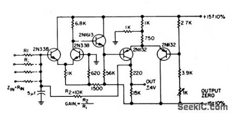
Uses current-summing to hold voltage at input node R1 at 0V. With more than one input, there is exact summation of inputs, with no interaction. As sine-wave amplifier, gain is 1,000, and bandwidth for transistors shown is d-c to 20kc.-C. J. Ulrick, Minimum. Interaction Summing Amplifier, EEE, 12:2, p 30. (View)
View full Circuit Diagram | Comments | Reading(1576)
SFERIC_SIMULATOR_CIRCUIT
Published:2009/7/15 0:14:00 Author:Jessie

This circuit generates a signal that simulates the waveform of a sferic-the very-low-frequency electromagnetic signals generated by a lightning strike. This circuit is designed to test and calibrate lightning-detecting instruments. Typically, lightning-detecting instruments have been calibrated and tested using single-frequency signals or broadband noise sources, which do not have the spectral characteristics of sferics. This circuit generates a bipolar pulse waveform that closely approximates the main features of sferics. The circuit contains few components. This circuit assembly is light in weight and compact; even a breadboard version could fit in a 1.5-inch square (about 3.8 cm). To ensure that the output waveform has the desired shape, the trigger pulse fed to the input terminal of this circuit must be a square wave with rise and fall times less than 100 ns. To prevent coalescence of sequential output pulses, the square-wave pulse-repetition frequency should be kept at or below 3000 Hz. (View)
View full Circuit Diagram | Comments | Reading(738)
MOBILE_AUTOPATCH
Published:2009/7/14 21:12:00 Author:May

Circuit operates push-to-talk of mobile station automatically when any button on Touch-Tone pad is pushed for dialing telephone number after making auto patch, eliminating need for engaging microphone before dialing. Circuit remains active for about 2 s after Touch-Tone button is released.-Circuits, 73 Magazine, May 1977. p 19. (View)
View full Circuit Diagram | Comments | Reading(1293)
| Pages:600/2234 At 20581582583584585586587588589590591592593594595596597598599600Under 20 |
Circuit Categories
power supply circuit
Amplifier Circuit
Basic Circuit
LED and Light Circuit
Sensor Circuit
Signal Processing
Electrical Equipment Circuit
Control Circuit
Remote Control Circuit
A/D-D/A Converter Circuit
Audio Circuit
Measuring and Test Circuit
Communication Circuit
Computer-Related Circuit
555 Circuit
Automotive Circuit
Repairing Circuit