
Circuit Diagram
Index 593
CMOS gate voltage-controlled oscillator circuit
Published:2011/8/6 3:26:00 Author:nelly | Keyword: CMOS, gate, voltage-controlled, oscillator

As it is shown in the figure, two non-gates A1 and A2 form the self-excited multivibrator. The oscillation frequency of the circuit will change with the size of the control voltage. When the value of Vcc is closed to the threshold, its influence to RC’s charge and discharge is the smallest, so the oscillation will be the lowest. When the Vcc is far from the threshold, the discharge and charge of the capacitor will be faster, so the oscillation will be higher.
(View)
View full Circuit Diagram | Comments | Reading(667)
Fast and synchronized voltage-controlled oscillator circuit
Published:2011/8/6 21:16:00 Author:nelly | Keyword: Fast, synchronized, voltage-controlled oscillator

This circuit is mainly used to connect the phase splitter and analog converter together, so the high-stable voltage-controlled oscillator and the external reference frequency can be synchronized precisely.
(View)
View full Circuit Diagram | Comments | Reading(601)
Voltage-controlled duty cycle oscillator circuit
Published:2011/8/7 4:14:00 Author:nelly | Keyword: Voltage-controlled, duty cycle, oscillator

The picture shows the self-excited multivibrator which is composed of 555 timer. FET VTl is used as the voltage-controlled resistor (VVR). Changing the voltage gate source VGS can alter the resistor between JEFT drain (D) and source (S). Two coupling capacitors can avoid the DC voltage of circuit’s other part from influencing VTl. In order not to make the coupling capacitor influence the charging and discharging time of 555 timer. The values of coupling capacitor C1 and C2 are ten times of timing capacitor, meanwhile, a resistance RDS can be achieved between the D pole and S pole of VTl.
(View)
View full Circuit Diagram | Comments | Reading(1528)
Voltage controlled oscillator (555) circuit with the logarithmic characteristic
Published:2011/8/6 2:29:00 Author:nelly | Keyword: voltage controlled, oscillator, logarithmic characteristic
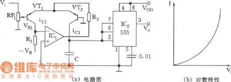
(a) circuit diagram (b)logarithmic characteristic (View)
View full Circuit Diagram | Comments | Reading(1125)
Exponential voltage-controlled oscillator (555) circuit
Published:2011/8/6 3:14:00 Author:nelly | Keyword: Exponential, voltage-controlled, oscillator
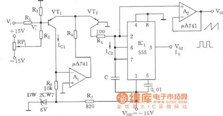

The relationship of Vi~555 oscillator frequency fo:
(View)
View full Circuit Diagram | Comments | Reading(1493)
Linear voltage-controlled oscillator (555) circuit
Published:2011/8/6 3:16:00 Author:nelly | Keyword: Linear, voltage-controlled, oscillator
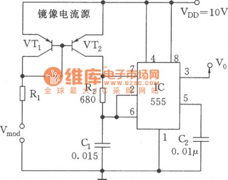
Linear voltage-controlled oscillator (555) circuit is as shown: (View)
View full Circuit Diagram | Comments | Reading(2866)
The voltage-controlled oscillator circuit with triangular and square wave output
Published:2011/8/6 21:43:00 Author:nelly | Keyword: voltage-controlled, oscillator, triangular wave, square wave

The figure shows the voltage-controlled oscillator circuit with triangular and square wave output. This circuit is the oscillator controlled by the voltage. It has the good stability and excellent linearity, and it also has the wide frequency range. This circuit has two output ends, one is the square wave output end, and the other is the triangle wave output end. In the picture, A1 is the inverter; A2 is the integrator; A3 is the comparator. FET Q1 is used to change the direction of integration. The reference voltage of the comparator is provided by the zener diode D1 and D2. (View)
View full Circuit Diagram | Comments | Reading(773)
The pulse generator circuit composed of CD4011
Published:2011/8/6 21:24:00 Author:nelly | Keyword: pulse generator

As shown in the picture, the logic pulse generator can transmit the negative or positive logic pulse, according to the need. This circuit is composed of a four-two input end and the non gate CD4011, among which D1 and D2 form a RS trigger pulse, and D3 and D4 are used as the inverters. It will be isolated with the D1 output end and drive a LED, thus the logic state of the output pulse can be indicated. (View)
View full Circuit Diagram | Comments | Reading(1494)
The pulse and pulse train generator circuit composed of CD4093
Published:2011/8/7 4:21:00 Author:nelly | Keyword: pulse, pulse train, generator

The pulse and pulse train generator is mainly composed of a four - two input Schmitt trigger CD4093 and a button switch. When the button is pressed, the circuit will output a single pulse. When the button is pressed for a period of time, the circuit will output the pulse train. The composition of the circuit is as shown in the picture. This circuit is composed of the button switch, input control circuit, pulse oscillator and pulse output circuit.
(View)
View full Circuit Diagram | Comments | Reading(2520)
VIDEO_MONITOR_TERMINATOR
Published:2009/7/14 21:43:00 Author:May
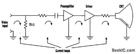
The best method of terminating video output signals is to route the video cable directly to the video-amplifier input connector without connecting its signal or shield wires to other parts of the monitor. (View)
View full Circuit Diagram | Comments | Reading(958)
INDEPENDENT_PULSE_WIDTH_CONTROL
Published:2009/7/14 21:42:00 Author:May

With components shown, circuit will divide 50-millisec pulses by 5 without changing pulse width. Other components give different widths along with division.-J. McGruder, Frequency Divider With Independent Pulse-Width Control, EEE, 14:2, p 69. (View)
View full Circuit Diagram | Comments | Reading(797)
VIDEO_INVERTER
Published:2009/7/14 21:42:00 Author:May

This video inverter circuit is based on an LM359 dual Norton op amp and an LM339 quad voltage comparator for dc restoration, sync detection and processing, and buffering and inversion of the video signal. The dc level of the video signal is restored to 0.7 V because the inputs of IC1-b operate at one diode voltage drop above ground. Comparator IC2-b acts as a threshold detector set to detect sync pulses 300 mV above the restored dc level of 0.7 V. Components C2 and R4 stretch the detected 4-μs sync pulses to 8μs to include the duration of 8 cycles of 3.58-MHz color burst after the input sync pulse. Comparators IC2-c and IC2-d buffer the stretched sync pulse with open-collector out-puts at pin 13 and 14 to gate the buffer/inverter action of the main amplifier IC1-a. Resistor R3 sets the gain of the inverting input of the main video amplifier IC1-a to 2 (-R1/R3= -2), and R4 sets the gain of the noninverting input of IC1-a to 4 (R1/R4=+4) These two inputs combine to achieve an overall gain of +2 as a buffer or -2 as an inverter. During the sync and color-burst portions of the in-put signal, the IC2-c and IC2-d outputs are open and the overall gain is +2. The rest of the time, a low at the output of IC2-d (pin 14) short-circuits the noninverting +4 signal path for an overall gain of -2, while a low at lC2-c pin 13 injects the necessary offset in the inverted video signal to keep it above the black level. Potentiometer R7 adjusts the black level at the output to correspond to the peak white level in the negative. Resistor R12 matches the output for 75Ω. A 78L05 regulator (IC3) provides a stable 5-V supply from a 9-V battery or ac adapter. (View)
View full Circuit Diagram | Comments | Reading(3324)
PULSE_FREQUENCY_DIVIDER_1
Published:2009/7/14 21:42:00 Author:May
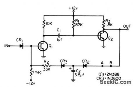
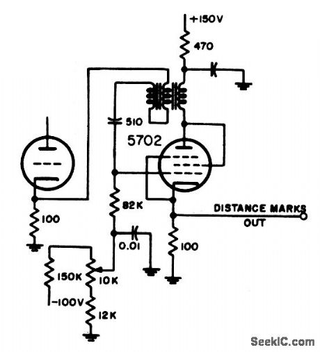
Plate-to-grid coupled blocking oscillator, with voltage step-up to grid, is used to divide from high to low pulse frequency.-NBS, Handbook Preferred Circuits Navy Aeronautical Electronic Equipment, Vol. 1, Electron Tube Circuits, 1963, p N7-1. (View)
View full Circuit Diagram | Comments | Reading(905)
PHANTASIRON_FREQUENCY_DIVIDER
Published:2009/7/14 21:40:00 Author:May
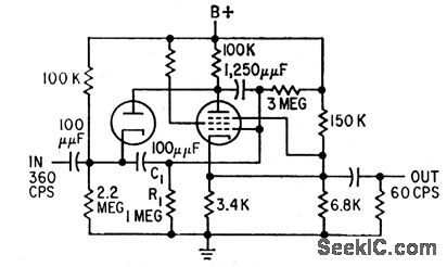
Will divide 360 cps to give 60 cps. Is triggered by pulse train with hoth positive and negative pulses.-K. M. Chen, Trigger Stabilizes Frequency Divider, Electronics, 31:47, p 104-107. (View)
View full Circuit Diagram | Comments | Reading(738)
VARIABLE_TURN_ON_AND_TURN_OFF
Published:2009/7/14 21:40:00 Author:May
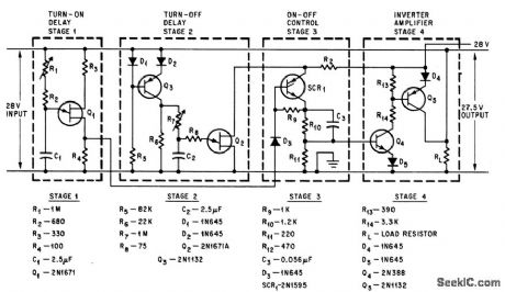
Both input and output delays are variable from 1.5 to 1,500 millisec. Maximum turn-on delay cannot exceed duration of input pulse. -C. R. Mora, Delay Circuit Varies Turn-on, Turn-off, Electronics, 39:7, p 92-93. (View)
View full Circuit Diagram | Comments | Reading(814)
RGB_SYNC_COMBINER_CIRCUIT
Published:2009/7/14 21:49:00 Author:Jessie

This circuit shows one way of combining RGB and sync signals from a computer to form an NTSC B/W video signal that is viewable on an ordinary video monitor.
(View)
View full Circuit Diagram | Comments | Reading(1944)
VIDEO_PATTERN_GENERATOR
Published:2009/7/14 21:47:00 Author:Jessie

A 3.58-MHz clock drives a counter chain, which addresses a preprogrammed EPROM, to generate a complete NTSC sync and video waveform. The EPROM can be programmed for various test patterns as required. A switch provides a choice of a checkerboard pattern, a color bar pattern, or a custom pattern. The total number of pixels in the custom pattern is 43,605. Each pixel can be programmed to one of the eight colors in the color bar pattern. The color signal is formed in the MC1377 encoder chip from the RGB digital inputs. The composite video out at PL1 is 2.5 V p-p. (View)
View full Circuit Diagram | Comments | Reading(1813)
500_MICROAMP_AT_30_TO_30000_CPS
Published:2009/7/14 21:47:00 Author:Jessie

Used to drive 60-mh transducer at constant current without allowing d-c through transducer. Achieved by biasing Q3 and Q4 on all the lime, so each acts as collector resistance for the other.-S. Sokol, Transistor Pair Provides Constant-Current Drive, Electronics, 35:38, p 56. (View)
View full Circuit Diagram | Comments | Reading(696)
PULSE_FREQUENCY_DIVIDER_3
Published:2009/7/14 21:46:00 Author:Jessie

Plate-to-cathode-to-grid coupled blocking oscillator is used to obtain high division ratios for pulses when stability of count is not too important. Lack of fixed bias means that this circuit will free-run in absence of input, but bias can be added if needed.-NBS, Handbook Preferred Circuits Navy Aeronautical Electronic Equipment, Vol. 1, Electron Tube Circuits, 1963, p N7-1. (View)
View full Circuit Diagram | Comments | Reading(684)
PULSE_FREQUENCY_DIVIDER_2
Published:2009/7/14 21:45:00 Author:Jessie
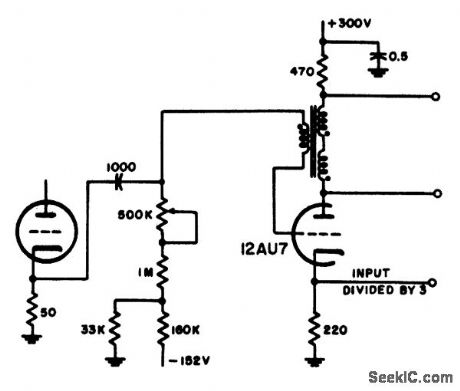
Plate-to-grid coupled blocking oscillator, with voltage step-down to grid, is used to divide from high to low pulse frequency. Stepdown yields maximum peak pulse voltage at plate and per mits maximum pulse duration from given transformer.-NBS, Handbook Preferred Circuits Navy Aeronautical Electronic Equipment, Vol. 1, Electron Tube Circuits, 1963, p N7-1. (View)
View full Circuit Diagram | Comments | Reading(861)
| Pages:593/2234 At 20581582583584585586587588589590591592593594595596597598599600Under 20 |
Circuit Categories
power supply circuit
Amplifier Circuit
Basic Circuit
LED and Light Circuit
Sensor Circuit
Signal Processing
Electrical Equipment Circuit
Control Circuit
Remote Control Circuit
A/D-D/A Converter Circuit
Audio Circuit
Measuring and Test Circuit
Communication Circuit
Computer-Related Circuit
555 Circuit
Automotive Circuit
Repairing Circuit