
Circuit Diagram
Index 584
farmland irrigation and drainage line anti-theft alarm(2)
Published:2011/7/20 5:14:00 Author:chopper | Keyword: farmland, irrigation and drainage line, anti-theft alarm

This example describes the farmland irrigation and drainage line anti-theft alarm, which controls the anti-theft alarm by detecting whether there is AC voltage of the each phase of the three-phase AC current or not.When the power line of farmland irrigation and drainage is stolen or the power outages,and phase lack of power line leads to a phase withoutAC voltage, the alarm will send an alarm signal in time. The principle of circuitThe farmland irrigation and drainage line anti-theft alarm is formed by the detection circuit,LED indication circuit and audible alarm circuit, which is shown in Figure 4-9. Detection circuit is formed by the test buttons S1-S3, resistors R1-R3, capacitors C1-Cl2 and diodes VD1-VD3, VD7, VD9, VD13-VD15.
(View)
View full Circuit Diagram | Comments | Reading(988)
farmland irrigation and drainage line anti-theft alarm(1)
Published:2011/7/20 5:01:00 Author:chopper | Keyword: farmland, irrigation and drainage line, anti-theft alarm

This example describes the farmland irrigation and drainage line anti-theft alarm.It can send out the alarm in time and point out the relevant line which is cut off when the power lineis in the destruction, which played a role in anti-theft protection. The principle of circuitThe farmland irrigation and drainage line anti-theft alarm circuit is formed by the detection circuit and sound alarm circuit, which is shown in Figure 4-93. Detection circuit is formed by the resistors R1-R12, LEDs VL1-VL3, transistors V1-V6.
(View)
View full Circuit Diagram | Comments | Reading(588)
monostable trigger circuit formed by gate circuit
Published:2011/7/22 3:01:00 Author:chopper | Keyword: monostable trigger, gate circuit


The CMOSnand-gate ornor-gate can form a monostable trigger, and this monostable trigger is used for the delay,broadening and shaping of the pulse signal extensively in the circuit.The main principle of monostable trigger with a gate circuit is to use the charge and discharge actions of the threshold level of gate input end and the component RC added to the gate circuit.Bothnand-gate or logic gate can form the monostable trigger,but their trigger modes are different,and the output logic levels are also different
.
(View)
View full Circuit Diagram | Comments | Reading(882)
slack delay monostable trigger with nand-gate
Published:2011/7/22 3:00:00 Author:chopper | Keyword: slack delay, monostable trigger, nand-gate


The picture shows aslackdelay monostable trigger with negative pulse trigger,and it provides a few seconds delay time for timing the situation whose accuracy is not critical. The delay in picture is mainly determined by capacitor C.As for TTL circuit,the resistance of R is generally 5~10kΩ. The table lists the measured data of delay when R = 5.1kΩ.The maximum capacity of C can reach several hundred microfarads, and delay can up to a few seconds.
(View)
View full Circuit Diagram | Comments | Reading(1438)
unique sound generating circuit with CD4040,CD4069
Published:2011/7/22 2:43:00 Author:chopper | Keyword: sound, generating circuit

The sound generating circuit can produce the sound which is similar to bird singing, car sirens and spacecraft sound,and it is a good toy for children.The circuit is shown in the picture.Core part is formed by a controlled oscillator composed of the gate circuit,which can change the oscillator frequency by adjusting the control voltage of the controlled oscillator, resulting in sending out a variety of analog sound. (View)
View full Circuit Diagram | Comments | Reading(3949)
quadruplex interlock switch circuit(1)(CD4028)circuit
Published:2011/7/20 23:11:00 Author:chopper | Keyword: quadruplex, interlock switch

View full Circuit Diagram | Comments | Reading(4460)
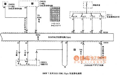
BMW7 Series EGS / EML 55pin Transmission Circuit (the 2nd)
Published:2011/7/17 21:43:00 Author:Felicity | Keyword: BMW7 Series, EGS / EML 55pin, Transmission Circuit, (the 2nd)
View full Circuit Diagram | Comments | Reading(1062)
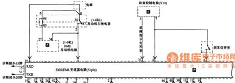
BMW7 Series EGS / EML 55pin Transmission Circuit (the 1st)
Published:2011/7/17 21:42:00 Author:Felicity | Keyword: BMW7 Series, EGS / EML 55pin, Transmission Circuit, (the 1st)
View full Circuit Diagram | Comments | Reading(965)
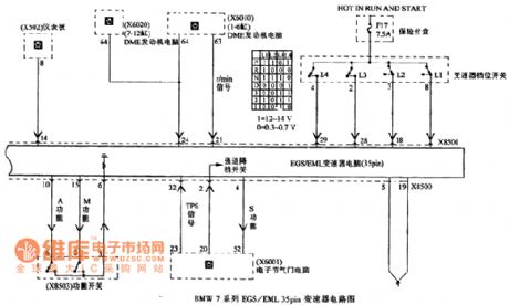
BMW7 Series EGS / EML 35pin Transmission Circuit (the 2nd)
Published:2011/7/17 21:50:00 Author:Felicity | Keyword: BMW7 Series, EGS / EML 35pin, Transmission Circuit, (the 2nd)
View full Circuit Diagram | Comments | Reading(984)
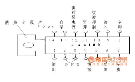
LA4100 Series Integrated Amplifier and Application Circuit
Published:2011/7/17 21:12:00 Author:Felicity | Keyword: LA4100 Series, Integrated, Amplifier, Application, Circuit
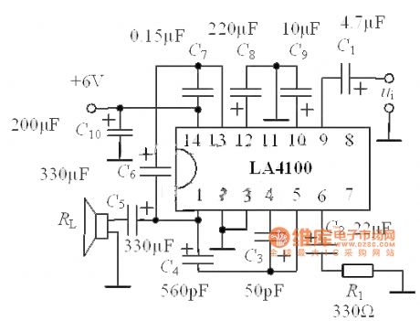
View full Circuit Diagram | Comments | Reading(3955)
The Circuit Diagram of 1 MHz High-pass Filter Consists of OPA603
Published:2011/8/8 7:54:00 Author:Felicity | Keyword: High-pass Filter

The figure shows the 1 MHz high-pass filter circuit. This circuit uses high speed current feedback operational amplifier OPA603 with 100MHz bandwidth and 1000V/μs slew rate. It is a second order Butterworth high-pass filter and the corner frequency f0=1/2πRC. Adopting the parameters shown in the figure, f0=1MHz and the circuit gain is 1.6. (View)
View full Circuit Diagram | Comments | Reading(1060)
The circuit diagram of notch filter consists of MC33171
Published:2011/8/8 6:51:00 Author:Felicity | Keyword: notch filter

The figure shows the notch filter circuit. This circuit uses high-performance amplifier MC33171 to build up notch filter. This component has wide bandwidth and high switching rate. The notch frequency can be changed by adjusting the value of R and C: f=1/4πRC. (View)
View full Circuit Diagram | Comments | Reading(869)
High-voltage Rectifier Circuit Of Side Thermal Rectifier Tube
Published:2011/7/17 20:56:00 Author:Felicity | Keyword: Side Thermal, Rectifier Tube, High-voltage Rectifier, Circuit
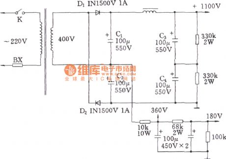
View full Circuit Diagram | Comments | Reading(1237)
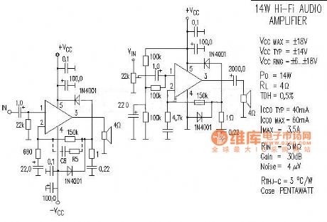
Power Amplifier Circuit
Published:2011/7/17 21:01:00 Author:Felicity | Keyword: Power Amplifier, Circuit
View full Circuit Diagram | Comments | Reading(1140)
The Circuit Diagram of One-hour Timing Circuit Using LM122
Published:2011/8/8 11:24:00 Author:Felicity | Keyword: Timing Circuit

In this figure S1 can start timing and when the timer starts, turning this switch has no effect.S2 is the “OFF” switch in the middle and turning this switch can make the timer complete the procedure: charging-open circuit-discharging. Because of charging stopped halfway, the charging position would return to the work state of the timer’s output circuit. And when C discharges, the voltage of R/C is zero and the charging position awaits the start signal of S1. (View)
View full Circuit Diagram | Comments | Reading(1843)
The circuit diagram of multiplication circuit 2 (MPY100)
Published:2011/8/6 0:14:00 Author:Felicity | Keyword: multiplication circuit


The increase of the factor of proportionality causes the Offset Voltage to rise, and this need zero modulation. Besides it can narrow the bandwidth. The figure shows the circuit diagram of multiplication circuit 2 (MPY100). Main parameters of MPY100: (View)
View full Circuit Diagram | Comments | Reading(691)
The Circuit Diagram of Active High-pass Filter (LM102)
Published:2011/8/8 11:29:00 Author:Felicity | Keyword: Active High-pass Filter

The figure shows the circuit diagram of active low-pass filter. The cutoff frequency fc=100Hz. In the circuit, the ratio of R1 to R2 or of C1 to C2 can be any value. In this circuit, R1=R2 and C1=2C2. C1=C2 and R1=2R2 can also be okay.
(View)
View full Circuit Diagram | Comments | Reading(2266)
Agricultural Irrigation Controller (the 2nd)
Published:2011/8/6 21:06:00 Author:Felicity | Keyword: Agricultural Irrigation, Controller

Work of the circuit
The circuit consists of power circuit, level detection control circuit and control implication circuit. (It is showed in picture 4-92.)
Power circuit consists of Buck capacitor Cl, discharge resistors Rl, rectifier diodes VDl, VD2, voltage regulator diode VS and filter capacitor C2.
Level detection control circuit consists of level detection electrodes a, b, resistors R2-R4, electronic integrated switching circuits and optical fused devices VLC.
Control implication circuit consists of Light garnet together control VLC, capacitor C3, resistor R5, bi-directional trigger diode V, VT and relay thyristor KA.
(View)
View full Circuit Diagram | Comments | Reading(584)
Agricultural Irrigation Controller (the 1st)
Published:2011/8/6 21:05:00 Author:Felicity | Keyword: Agricultural Irrigation, Controller

Work of the circuit
The circuit consists of power circuit and level detection control circuit. (It is showed in picture 4-91.)
Power circuit consists of fuse FU, power transformer T, bridge rectifier, UR, filter capacitors Cl, C2, limiting resistors R3 and integrated three-terminal regulator IC.
Level detection control circuit consists of high water level electrode A, the low water level electrode B, the main electrode C, resistors Rl, R2, transistor V, Relay K, diode VD and AC contactor KM.
(View)
View full Circuit Diagram | Comments | Reading(745)
The centralized controller of drainage and irrigation pumping station One
Published:2011/8/8 20:33:00 Author:Felicity | Keyword: drainage and irrigation pumping station , centralized controller,

When the control room starts, the switch Q turns on. After S1 is pressed ,the phase voltage of L2 goes through S1,R1,signal line a, normally close contact of KM,KA (to null line N or ground) to make up current circuit. And KA turns on and closes, and the normally open contact KA1 switched on, the normally closed contact M2 switched off. And the phase voltage goes to phase L3 to form a circuit. After fast discharging of K, the inner contact closes to make KM turns on, and the normally open contact closes, the pump motor starting. (View)
View full Circuit Diagram | Comments | Reading(865)
| Pages:584/2234 At 20581582583584585586587588589590591592593594595596597598599600Under 20 |
Circuit Categories
power supply circuit
Amplifier Circuit
Basic Circuit
LED and Light Circuit
Sensor Circuit
Signal Processing
Electrical Equipment Circuit
Control Circuit
Remote Control Circuit
A/D-D/A Converter Circuit
Audio Circuit
Measuring and Test Circuit
Communication Circuit
Computer-Related Circuit
555 Circuit
Automotive Circuit
Repairing Circuit